
Electric-thermal separated, LED chip integrated and high-reflectivity circuit board and manufacture method thereof

A LED chip, electrothermal separation technology, applied in the direction of printed circuits, circuits, and electrical components connected with non-printed electrical components, can solve the problems of occlusion, reduced luminous efficiency, and reduced thermal conductivity, so as to increase luminous efficiency, improve Luminous efficiency, cost saving effect

Inactive Publication Date: 2016-01-27
XIAMEN HUIGENG ELECTRONICS IND
View PDF4 Cites 0 Cited by
  • Summary
  • Abstract
  • Description
  • Claims
  • Application Information

AI Technical Summary

Problems solved by technology

In the traditional process, the LED substrate is divided into aluminum layer, insulating layer and copper foil layer; copper and aluminum have good thermal conductivity as metal materials, but due to the existence of the insulating layer, the thermal conductivity of these two materials is greatly reduced, so As a result, the heat generated by the LED chip cannot be dissipated in time, and the long-term high temperature seriously shortens the life of the LED chip
[0003] At the same time, in the traditional LED manufacturing process, each LED core needs to be connected to the positive and negative poles and packaged separately, which increases the production cost, and the positive and negative poles will block the light emitted by a part of the LED chip, resulting in a decrease in luminous efficiency.
[0004] In addition, in the traditional LED manufacturing process, epoxy resin coating is used to reflect the light emitted by the LED chip, but the reflection efficiency of the epoxy resin coating is low, and it will absorb the light emitted by a LED chip, resulting in the traditional LED chip Luminous efficiency is not high

Method used


Image

  • Electric-thermal separated, LED chip integrated and high-reflectivity circuit board and manufacture method thereof
  • Electric-thermal separated, LED chip integrated and high-reflectivity circuit board and manufacture method thereof

Examples


Embodiment Construction

[0026] Hereinafter, the present invention will be further described with reference to the drawings and specific embodiments.

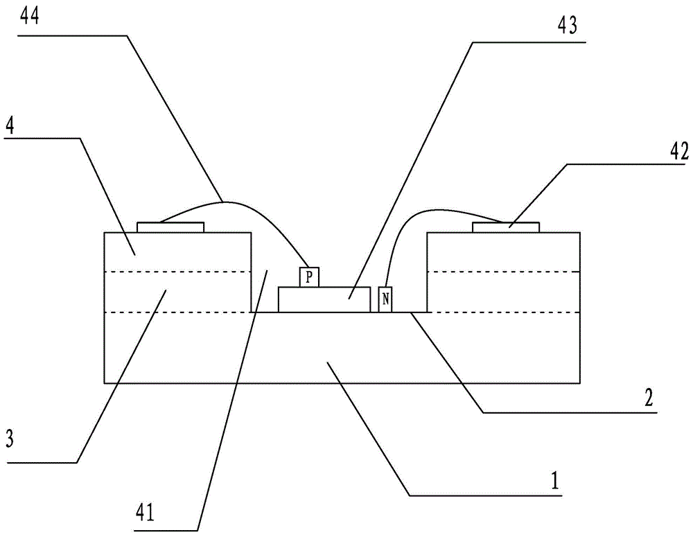
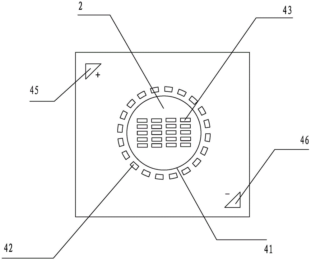
[0027] reference figure 1 , figure 2 . High-reflectivity circuit board with electrothermal separation and integration of LED chips, including:

[0028] The heat dissipation layer 1, the insulating layer 3, and the circuit layer 4 are laminated in sequence; the side of the heat dissipation layer 1 that contacts the insulating layer 3 is mirror aluminum 2; the circuit layer 4 is provided with at least one connected to the mirror aluminum 2 hole 41; in this embodiment, the material of the circuit layer 4 is copper foil; the material of the insulating layer 3 is epoxy.

[0029] At least one LED chip 43 is mounted on the mirror aluminum 2 located in the hole 41;

[0030] At least one LED solder joint 42 is provided on the circuit layer, and the LED solder joints 42 are independent of each other and arranged outside the hole 41; the P pole and the N pole of the L...


PUM


Abstract

The invention relates to an electric-thermal separated, LED chip integrated and high-reflectivity circuit board. The circuit comprises a heat radiation layer, an insulating layer and a circuit layer, wherein the heat radiation layer, the insulating layer and the circuit layer are laminated successively, the side where the heat radiation layer makes contact with the insulating layer includes minute surface aluminum, the circuit layer includes at least one slot communicated with the minute surface aluminum, the minute surface aluminum placed in the slot is provided with at least one LED chip, the circuit layer is provided with at least one LED welding point, the LED welding points are independent from each other and arranged outside the slot, poles P and N of the LED chip are connected to the LED welding point via gold threads respectively, the circuit layer is further provided with an anode and a cathode, and the anode and the cathode are connected with LED welding points via circuits respectively.

Description

Technical field [0001] The invention relates to the field of LED manufacturing, in particular to an LED circuit board. Background technique [0002] With the advancement of LED technology, heat dissipation has become an important bottleneck restricting the continued development of LED technology. In the traditional process, the LED substrate is divided into aluminum layer, insulating layer and copper foil layer; copper and aluminum have good thermal conductivity as metal materials, but due to the existence of the insulating layer, the thermal conductivity of these two materials is greatly reduced, so As a result, the heat generated by the LED chip cannot be dissipated in time, and the long-term high temperature seriously shortens the life of the LED chip. [0003] At the same time, in the traditional LED manufacturing process, each LED core needs to be individually packaged after being connected to the positive and negative electrodes, resulting in an increase in manufacturing cos...

Claims


Application Information

Patent Timeline
Patent Type & Authority Applications(China)
IPC IPC(8): H01L33/62H05K1/18
CPCH01L2224/48091
Inventor 陈诺成
Owner XIAMEN HUIGENG ELECTRONICS IND
Learn More