

Hearing aid interface circuit and method
An interface and circuit technology, applied in hearing aids, instruments, electrical components, etc., can solve the problem of chip consumption, and achieve the effect of high driving strength and low dynamic power consumption
- Summary
- Abstract
- Description
- Claims
- Application Information
AI Technical Summary
Problems solved by technology
Method used
Image

Examples
Embodiment Construction
[0044] Various features are described below with reference to the accompanying drawings. It should be noted that the figures may or may not be drawn to scale, and that elements of similar structure or function are represented by like reference numerals throughout the figures. It should be noted that the drawings are only intended to aid in describing the features. They are not intended as an exhaustive description of or as a limitation on the scope of the claimed invention. Additionally, an illustrated feature need not have all of the aspects or advantages shown. An aspect or advantage described in connection with a particular feature is not necessarily limited to that feature and may be practiced with any other feature even if not so stated or so explicitly described.
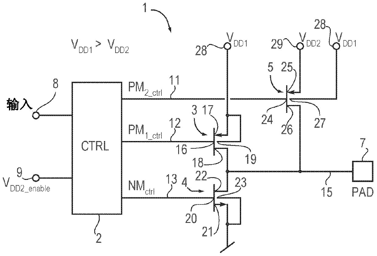
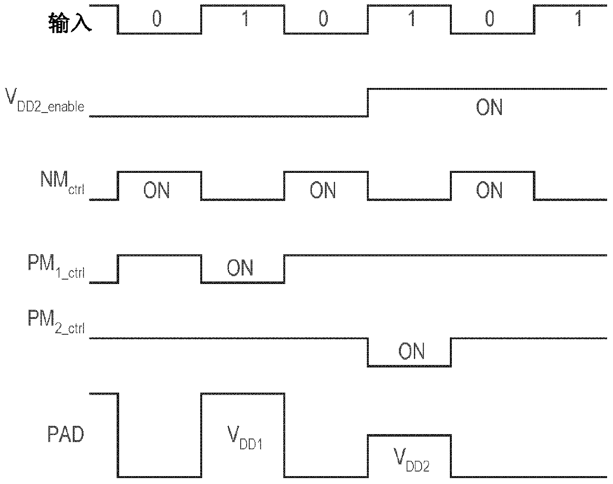
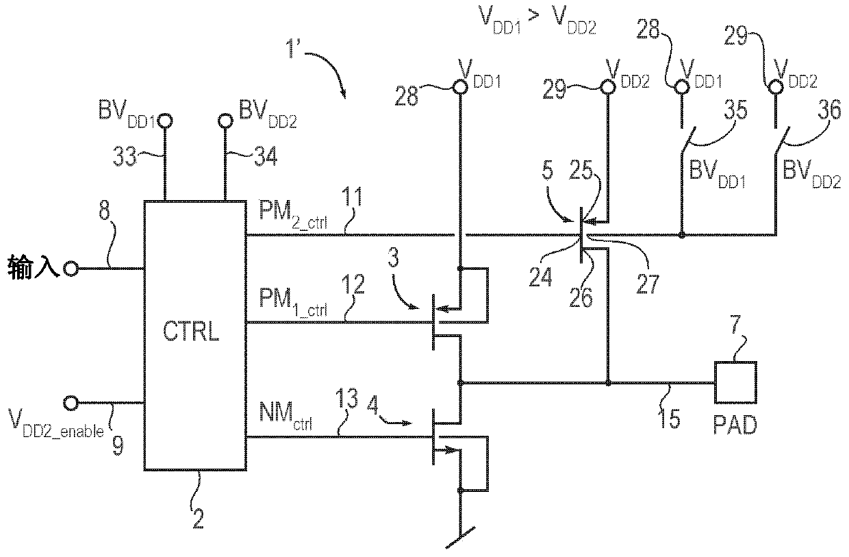
[0045] figure 1 It is a schematic diagram showing the main components of the interface pad circuit 1 for the microelectronic chip of the hearing aid according to the first embodiment. The interface pad cir...
PUM
 Abstract
Description
Claims
Application Information