Wafer gumming machine and gumming method

A technology of gluing machine and wafer, which is applied in the direction of coating, device for coating liquid on the surface, electrical components, etc., to achieve the effect of widening the scope

Inactive Publication Date: 2016-02-03
ACM RES SHANGHAI
View PDF5 Cites 20 Cited by
  • Summary
  • Abstract
  • Description
  • Claims
  • Application Information

AI Technical Summary

Problems solved by technology

However, in the existing industry structure, few manufacturers can produce gluing machines that are compatible with wafers of different sizes at the same time and do not affect each other during the gluing process.

Method used


Image

  • Wafer gumming machine and gumming method
  • Wafer gumming machine and gumming method
  • Wafer gumming machine and gumming method

Examples


Embodiment Construction

[0040] The following further description of the specific embodiments and implementations in conjunction with the accompanying drawings can help those skilled in the art to fully and effectively understand the essential content of the present invention, so as to achieve the repeated realization of the technical solution under the condition of knowing the patent content of the present invention Degree.

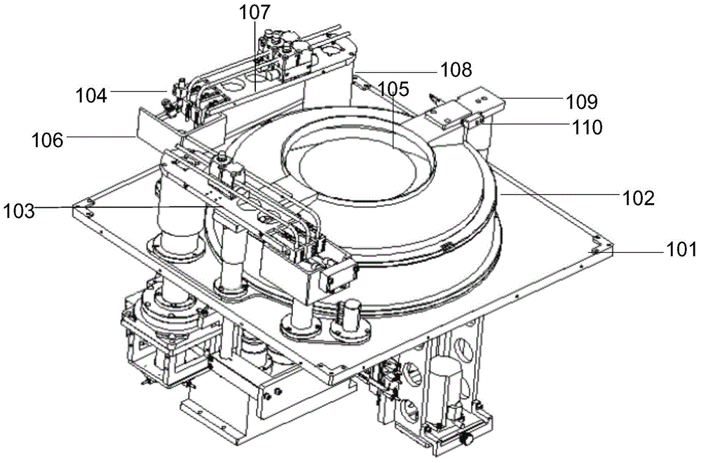
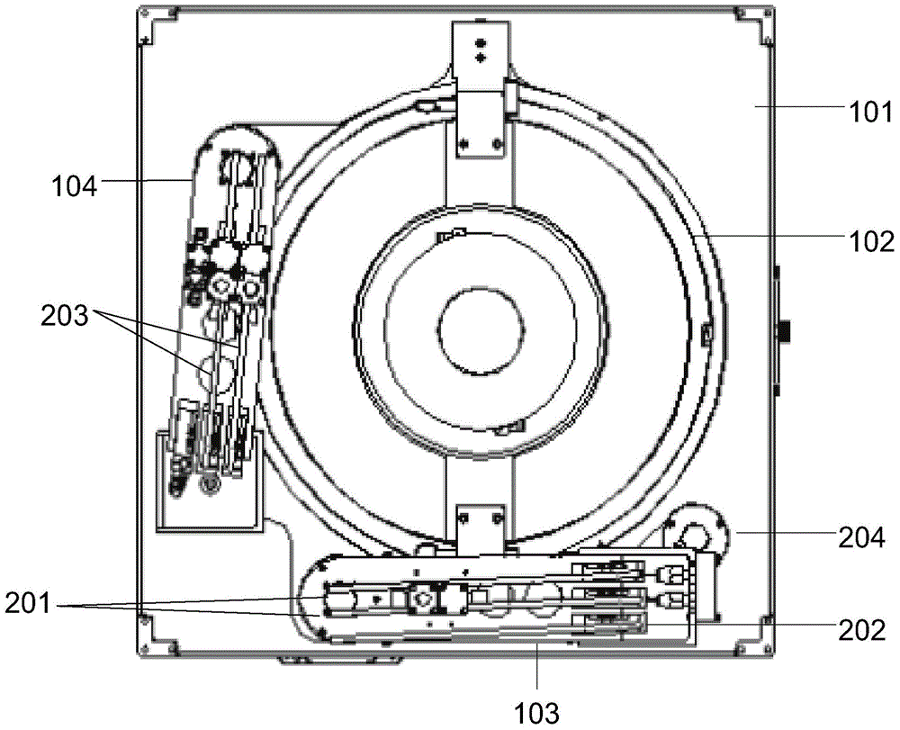
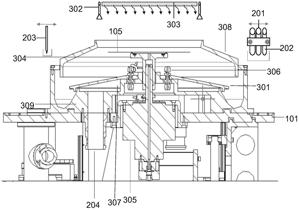
[0041] See attached Figure 1-3 , you will know the structural information of the wafer gluing machine of the present invention and understand the connection relationship between the various components.

[0042] in, figure 1 The overall display of the wafer gluing machine is made, figure 2 and image 3 The structural features of the wafer gluing machine are given in two different dimensions from the top and the side, respectively.

[0043] Specifically, the wafer gluing machine has a process chamber 100, the process chamber 100 constitutes a closed process space, and the fo...


PUM


Abstract

The invention relates to a wafer gumming machine and a gumming method. The wafer gumming machine can carry out gumming on wafers of different sizes. The wafer gumming machine is provided with at least one technological cavity. A cavity cleaning nozzle is arranged at the top of the technological cavity so that the wafer gumming machine can be automatically cleaned without starting the machine, and the time cost and manpower cost consumed by machine table cleaning are greatly saved. The gumming method suitable for the wafer gumming machine is further provided. A good gumming effect is achieved.

Description

technical field [0001] The invention relates to the field of semiconductor production and manufacture, in particular to a wafer gluing machine and a gluing method. Background technique [0002] In the semiconductor device manufacturing and advanced packaging process, the lithography process refers to the process of photoresist coating, exposure, and development on a substrate, such as a semiconductor wafer, in order to design a photolithography mask (MASK). The process of transferring the pattern to the film layer on the surface of the substrate. During the photoresist coating process, a photoresist film layer is formed by applying a photoresist solution on the surface of the substrate and heating the applied photoresist solution, and then photolithography on the surface of the substrate is performed by an exposure and development process. A prescribed pattern structure is formed in the adhesive layer. In the above-mentioned photoresist coating process, the wafer is genera...

Claims


Application Information

Patent Timeline
Patent Type & Authority Applications(China)
IPC IPC(8): B05C5/00B05C11/00B05C11/08B05C13/02B05C15/00H01L21/67
Inventor 王文军王晖陈福平张怀东
Owner ACM RES SHANGHAI
Why Eureka
Try Eureka