Induction device applicable to wafer photolithography process

A lithography process and sensing device technology, which is applied to the sensing device field of wafer lithography process, can solve the problems of uncertainty of reflection angle, rough surface of wafer, difficult to guarantee sensing accuracy, etc. The effect of precision improvement

Inactive Publication Date: 2016-02-10
SUZHOU SAISEN ELECTRONICS TECH
View PDF4 Cites 0 Cited by
  • Summary
  • Abstract
  • Description
  • Claims
  • Application Information

AI Technical Summary

Problems solved by technology

However, due to the rough surface of the wafer, especially the wafer to be processed, there is uncertainty in the reflection angle, which makes it difficult to guarantee the sensing accuracy, which often leads to debris during the processing

Method used


Image

  • Induction device applicable to wafer photolithography process

Examples


Embodiment 1

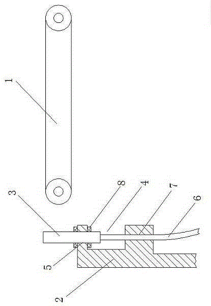
[0014] like figure 1 A kind of induction device suitable for wafer lithography process is shown, and it comprises the feeding device 1 that is used for transferring wafer; The front end portion of described feeding device 1 is provided with induction support 2, and A proximity switch 3 is arranged on the top, and the proximity switch 3 and the feeding device 1 are opposite to each other.

[0015] As an improvement of the present invention, a placement tank 4 is provided on the opposite end surface of the induction bracket 2 and the feeding device 1, and the upper end surface of the placement tank 4 is provided with a placement hole 5, and the proximity switch 3 is installed The hole 4 is connected to the induction bracket 2 , and the lower end of the proximity switch 3 extends to the interior of the placement tank 4 . With the above design, it can form the installation position corresponding to the proximity switch through the setting of the placement groove in the induction ...

Embodiment 2

[0019] As an improvement of the present invention, the connection positions between the proximity switch 3 and the upper and lower ends of the placement hole 5 are respectively provided with rubber damping rings 8, which can prevent the proximity switch from falling or even being damaged due to factors such as mechanical vibration, thereby The service life of the induction device is improved.

[0020] The remaining features and advantages of this embodiment are the same as those of Embodiment 1.


PUM


Abstract

The invention discloses an induction device applicable to a wafer photolithography process. The induction device comprises a feeding device, wherein the feeding device is used for transmitting a wafer; an induction bracket is arranged at the front end part of the feeding device; and a proximity switch is arranged on the induction bracket and is opposite to the feeding device. By the induction device applicable to the wafer photolithography process disclosed by the technical scheme, photoelectric induction adopted by a conventional disk induction device can be replaced through the proximity switch, so that the induction device is not affected by the surface roughness of the wafer; the induction accuracy is improved; and the fragment phenomenon in the processing process is significantly improved.

Description

technical field [0001] The invention relates to a semiconductor processing device, in particular to an induction device suitable for a wafer photolithography process. Background technique [0002] During photolithography processing, it is often necessary to judge the position of the wafer to be processed before processing. The traditional wafer position sensing uses a photoelectric sensing device, that is, two symmetrically distributed light generators and receivers are used to sense the position of the wafer through the reflection of light on the wafer surface. However, due to the rough surface of the wafer, especially the wafer to be processed, there is uncertainty in the reflection angle, which makes it difficult to guarantee the sensing accuracy, which often leads to debris during the processing process. Contents of the invention [0003] The technical problem to be solved by the present invention is to provide a sensing device suitable for a wafer photolithography pr...

Claims


Application Information

Patent Timeline
Patent Type & Authority Applications(China)
IPC IPC(8): G03F7/20
Inventor 史进伍志军
Owner SUZHOU SAISEN ELECTRONICS TECH
Why Eureka
Try Eureka