Fingerprint identification chip and manufacturing method therefor

A fingerprint identification and manufacturing method technology, which is applied in character and pattern recognition, semiconductor/solid-state device manufacturing, instruments, etc., can solve the problems that the sensitivity of fingerprint identification cannot be improved to the best state, so as to improve the sensitivity, reduce the distance, and shorten the distance Effect

Inactive Publication Date: 2016-02-17
SEMICON MFG INT (SHANGHAI) CORP
View PDF5 Cites 4 Cited by
  • Summary
  • Abstract
  • Description
  • Claims
  • Application Information

AI Technical Summary

Problems solved by technology

[0004] The purpose of the present invention is to provide a fingerprint identification chip and its manufacturing method, to solve the problem that the method for improving the sensitivity of fingerprint identification of the fingerprint identification chip in the prior art still has deficiencies, and the sensitivity of fingerprint identification cannot be raised to the best state. question

Method used


Image

  • Fingerprint identification chip and manufacturing method therefor
  • Fingerprint identification chip and manufacturing method therefor
  • Fingerprint identification chip and manufacturing method therefor

Examples


Embodiment Construction

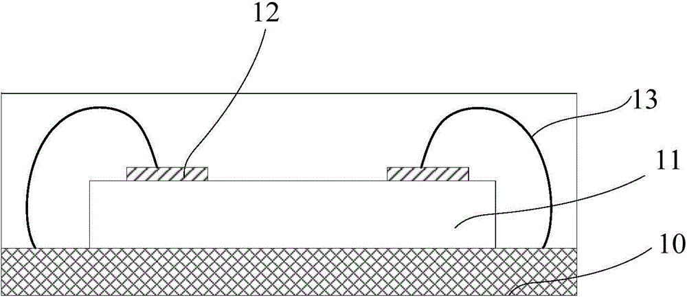
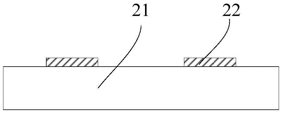
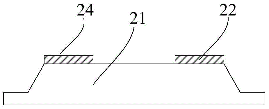
[0031] The fingerprint identification chip proposed by the present invention and its manufacturing method will be further described in detail below in conjunction with the accompanying drawings and specific embodiments. Advantages and features of the present invention will be apparent from the following description and claims. It should be noted that all the drawings are in a very simplified form and use imprecise scales, and are only used to facilitate and clearly assist the purpose of illustrating the embodiments of the present invention.

[0032] This embodiment provides a method for manufacturing a fingerprint recognition chip. Refer below Figures 2A-2F and image 3 . in, Figures 2A-2F It is a schematic cross-sectional view of each step in the manufacturing method of the fingerprint identification chip in an embodiment of the present invention; image 3 It is a flowchart of a method for manufacturing a fingerprint identification chip according to an embodiment of th...


PUM


Abstract

The invention provides a fingerprint identification chip and a manufacturing method therefor. The fingerprint identification chip comprises a substrate, a wafer arranged on the substrate, a sensing unit integrated on a first surface of the wafer, and a conductive layer, wherein a groove is formed in the edge of the wafer; the bottom of the groove is lower than the first surface of the wafer in a vertical direction; the sensing unit is connected with the substrate in a binding manner through a binding line; and one end of the conductive layer is connected with the sensing unit, and the other end of the conductive layer extends to the bottom of the groove. The groove structure is formed in the edge of the wafer, and one end, connected with the sensing unit, of the binding line is pulled down through the conductive layer arranged on the groove wall of the groove, so that the distance from the sensing unit to the top end of the fingerprint identification chip is reduced, the distance between the sensing unit and a finger of a user is shortened, and the sensitivity of the fingerprint identification chip is improved.

Description

technical field [0001] The invention relates to the technical field of integrated circuits, in particular to a fingerprint recognition chip and a manufacturing method thereof. Background technique [0002] Please refer to figure 1 , which is a cross-sectional view of a fingerprint identification chip in the prior art, such as figure 1 As shown, the existing fingerprint identification chip includes a substrate 10, a wafer 11 disposed on the base 10, and a sensing unit 12 integrated on the wafer 11, and the substrate 10 and the sensing unit 12 are realized by bonding wires 13. connect. The sensing unit 12 is used to extract the user's fingerprint information, and its application principle is to image the fingerprint by measuring the difference in the coupling capacitance formed between the fingerprint ridge line and the valley line and the sensing electrode array unit of the sensing unit. of. In order to improve the sensitivity of the fingerprint identification chip, so th...

Claims


Application Information

Patent Timeline
Patent Type & Authority Applications(China)
IPC IPC(8): G06K9/00H01L21/98
CPCH01L2224/05H01L2224/48091H01L2924/10155H01L2924/00014
Inventor 施森华胡王凯魏磊
Owner SEMICON MFG INT (SHANGHAI) CORP
Why Eureka
Try Eureka