Packaging structure for transferring chip bonding stress and production method thereof

A technology for mounting stress and transferring chips, applied in microstructure technology, microstructure devices, manufacturing microstructure devices, etc., can solve the problems of communication with the external environment, high vacuum degree, etc., to reduce the impact and reduce the thermal expansion coefficient. Effect

Inactive Publication Date: 2016-02-24
HUATIAN TECH KUNSHAN ELECTRONICS
View PDF5 Cites 5 Cited by
  • Summary
  • Abstract
  • Description
  • Claims
  • Application Information

AI Technical Summary

Problems solved by technology

[0003] After decades of technological development, some MEMS chips with high demand have been quite mature, but because the unique movable/sensitive structure of MEMS devices puts forward higher requirements for packaging, it is necessary to reduce the impact of the packaging process on the packaged chips At...

Method used


Image

  • Packaging structure for transferring chip bonding stress and production method thereof
  • Packaging structure for transferring chip bonding stress and production method thereof
  • Packaging structure for transferring chip bonding stress and production method thereof

Examples


Embodiment Construction

[0042] In order to understand the technical content of the present invention more clearly, the following examples are given in detail, the purpose of which is only to better understand the content of the present invention but not to limit the protection scope of the present invention. For convenience of description, the components in the structures in the drawings of the embodiments are not scaled according to the normal scale, so they do not represent the actual relative sizes of the structures in the embodiments.

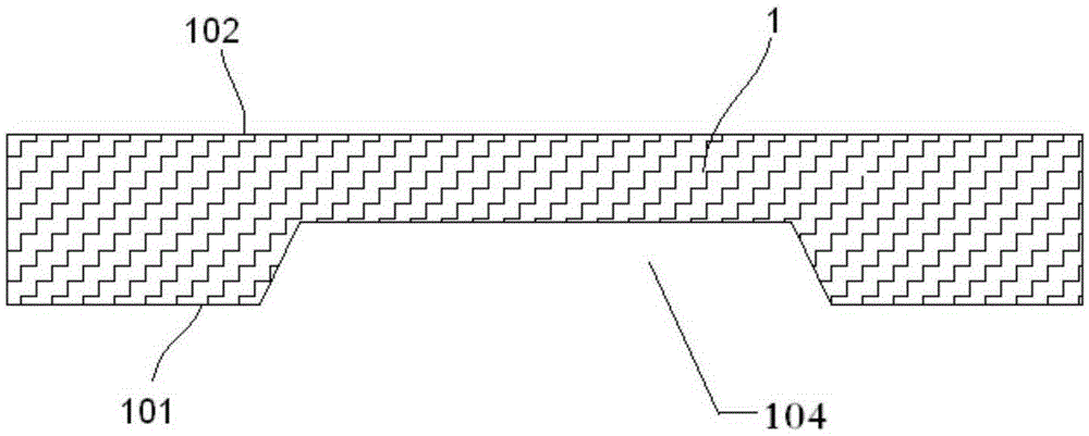
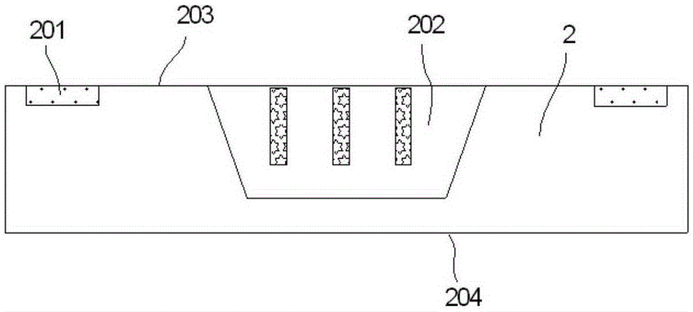
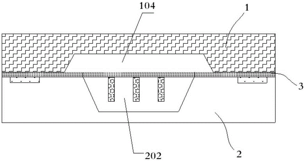
[0043] Such as Figure 7 As shown, a packaging structure for transferring chip mounting stress includes a functional chip 2 and a cover plate 1. The front side of the functional chip is a functional surface, and the functional surface has a functional area 202 and a surrounding area of ​​the functional area. Several conductive pads 201, the cover plate has a first surface 101 and a second surface 102 opposite to it; the first surface of the cover plate is bonded t...


PUM


Abstract

The invention discloses a packaging structure for transferring chip bonding stress and a production method thereof. The packaging structure comprises a functional chip and a cover board made of the same material as a substrate thereof, wherein a function surface of the functional chip is provided with a functional zone and a plurality of conductive welding pads arranged at the periphery of the functional zone; the cover board is provided with a first surface with a cavity and a second surface opposite to the first surface; the first surface of the cover board is bonded with the function surface of the functional chip; the second surface of the cover board is subjected to re-wiring to form a metal line layer which extends to the conductive welding pads; and a metal line cannot extend to a cutting path position. Through changing the previous design structure adopting chip back wiring to a design structure adopting front wiring, the influence of the stress which is generated by back operation on the chip functional zone is reduced; and furthermore, the material of which the substrate of the functional chip is made is used to make the cover board and wiring is carried out on the cover board, so that a problem of mismatching of a coefficient of thermal expansion between the cover board and the chip is avoided, and the packaging process steps are simple.

Description

technical field [0001] The invention relates to a wafer-level chip package, in particular to a package structure for transferring chip mounting stress and a manufacturing method thereof. Background technique [0002] Micro Electro Mechanical Systems (MEMS: Micro Electro Mechanical Systems) is a new type of multidisciplinary cutting-edge technology developed since the 1980s. The combination of processing technology and micromachining technology in the mechanical industry produces various sensors, actuators, drives and microsystems with excellent performance, low price and miniaturization. Due to its miniaturization advantages, MEMS has broad application prospects in electronics, automobiles, electromechanical, sensors, military and other fields. Currently commercialized MEMS devices include inertial devices (gyroscopes, accelerometers, etc.), RF devices, and pressure sensors. , Microphone, Micro-mirror, etc. [0003] After decades of technological development, some MEMS chi...

Claims


Application Information

Patent Timeline
IPC IPC(8): B81B7/00B81C1/00
CPCB81B7/0032B81B7/007B81C1/00269B81C1/00301
Inventor 万里兮袁礼明豆菲菲翟玲玲
Owner HUATIAN TECH KUNSHAN ELECTRONICS
Why Eureka
Try Eureka