Quantum well combined LED epitaxial structure with high luminous efficiency and its preparation method
A technology with high luminous efficiency and multiple quantum well structure, applied in electrical components, circuits, semiconductor devices, etc., can solve the problems of high stress and low efficiency, and achieve the effects of reducing stress, improving device performance, and improving light extraction efficiency.
- Summary
- Abstract
- Description
- Claims
- Application Information
AI Technical Summary
Problems solved by technology
Method used
Image
Examples
Embodiment Construction
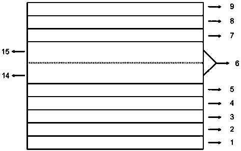
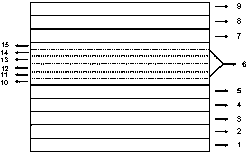
[0049] figure 2 The quantum well combination LED epitaxial structure with high luminous efficiency of the present invention is given, which can effectively reduce the stress between the well-barrier interface, alleviate the bending of the energy band, and improve the efficiency of hole and electron injection into the active region and the efficiency of radiation recombination. The epitaxial structure is substrate 1, buffer layer 2, undoped GaN layer 3, n-type AlGaN layer 4, n-type GaN layer 5, active layer 6, p-type AlGaN layer 7, p-type GaN layer from bottom to top 8 and P-type InGaN contact layer 9, with figure 1 The difference of the existing structures shown is that the active layer 6 includes a lower multi-quantum well structure, a constant temperature multi-quantum well structure and an upper multi-quantum well structure, and the lower multi-quantum well structure is an InxGa1-xN potential well layer 10 (0
PUM
 Abstract
Description
Claims
Application Information


