Formation method of semiconductor device

A semiconductor and device technology, applied in the field of semiconductor device formation, can solve problems such as low yield, poor reliability, and poor reliability of semiconductor devices, and achieve the effects of improving production efficiency, increasing distance, and reducing contact resistance

Active Publication Date: 2016-03-02
SEMICON MFG INT (SHANGHAI) CORP
View PDF8 Cites 5 Cited by
  • Summary
  • Abstract
  • Description
  • Claims
  • Application Information

AI Technical Summary

Problems solved by technology

[0005] However, with the continuous shrinking of the size of semiconductor structures, the formed semiconductor devices have problems of poor reliability and low yield, espec

Method used


Image

  • Formation method of semiconductor device
  • Formation method of semiconductor device
  • Formation method of semiconductor device

Examples


Example Embodiment

[0036] It can be known from the background art that semiconductor devices formed in the prior art have the problems of poor reliability and low yield.

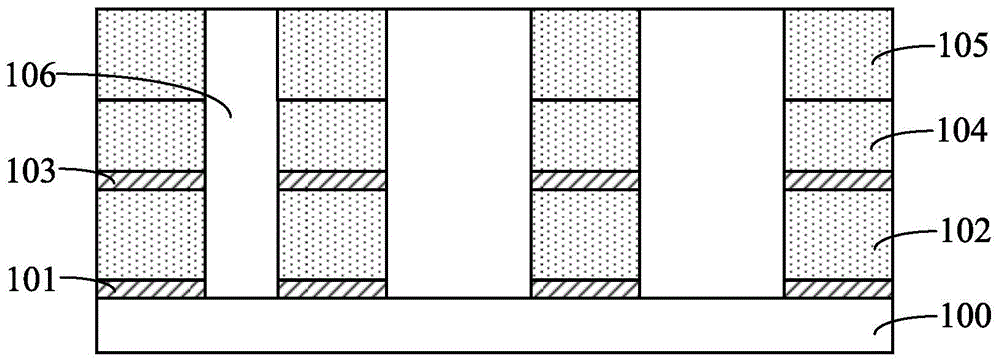
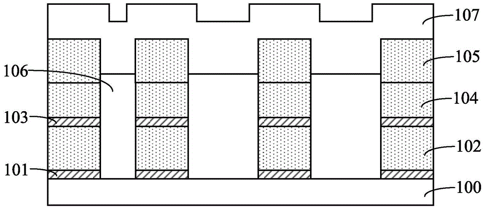
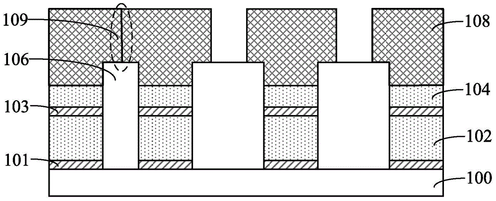
[0037] The method of forming a metal contact layer on the surface of the gate structure is studied. The process steps for forming the metal contact layer include: forming a metal layer on the surface of the gate structure; annealing the metal layer, and the metal layer material and the gate structure material A silicidation reaction occurs, forming a metal contact layer on the surface of the gate structure; removing the unreacted metal layer.

[0038] Since the thickness of the metal silicide layer is thicker, the effect of reducing the contact resistance of the semiconductor device is better. Especially for flash memory devices, since the control gate conductive layer has a relatively thick thickness, the thickness of the metal contact layer is required to be thicker. To reduce the contact resistance of semiconductor devices. To ...


PUM


Abstract

Provided is a formation method of a semiconductor device. The formation method includes: a substrate with is provided, grid electrode structures are formed on the surface of the substrate, a semiconductor material layer is formed on the surface of the top of each grid electrode structure, and sidewalls of the grid electrode structure are aligned with sidewalls of the semiconductor material layer; an interlayer dielectric layer is formed on the surface of the substrate; the interlayer dielectric layer with certain thickness is removed via etching, and surfaces of the sidewalls of the semiconductor material layer are exposed; oxidation treatment of the surfaces of the sidewalls of the semiconductor material layer is performed, and the semiconductor material layer with certain width is converted to a sacrificial layer; the sacrificial layer is removed; a metal layer is formed on the surface of the top and the surfaces of the sidewalls of the remaining semiconductor material layer; and annealing treatment of the metal layer is performed, the metal layer reacts with the remaining semiconductor material layer, and a metal contact layer is formed on the surface of the top of each grid electrode structure. According to the formation method, the metal contact layers are additionally provided so that over-short distance or mutual contact of the adjacent metal contact layers are prevented, and the reliability and the yield of the semiconductor device are increased.

Description

technical field [0001] The invention relates to the technology in the field of semiconductor manufacturing, in particular to a method for forming a semiconductor device. Background technique [0002] With the continuous increase of the integration level of semiconductor devices, the critical dimensions of semiconductor devices are continuously reduced, and many problems have appeared correspondingly, such as the corresponding increase in surface resistance and contact resistance of the drain, source and gate structures of semiconductor devices, resulting in the decrease of semiconductor devices. The response speed is reduced and the signal is delayed. Therefore, an interconnection structure with low resistivity becomes a key element in the manufacture of highly integrated semiconductor devices. [0003] In order to reduce the contact resistance of the drain-source and gate structures of semiconductor devices, the process method of metal silicide is introduced. The metal sil...

Claims


Application Information

Patent Timeline
IPC IPC(8): H01L21/768
Inventor 刘佳磊
Owner SEMICON MFG INT (SHANGHAI) CORP
Why Eureka
Try Eureka