Circuit board and manufacturing method of the circuit board

A manufacturing method and circuit board technology, applied in the directions of printed circuit components, secondary processing of printed circuits, and electrical connection of printed components, etc., can solve problems such as poor gold deposition, and achieve the effect of improving the reaction rate and improving poor gold deposition.

Active Publication Date: 2016-03-02
AVARY HLDG (SHENZHEN) CO LTD +1
View PDF4 Cites 2 Cited by
  • Summary
  • Abstract
  • Description
  • Claims
  • Application Information

AI Technical Summary

Problems solved by technology

[0003] In view of this, it is necessary to provide a circuit board that can improve problems such as poor gold plating in the gold chemical process

Method used


Image

  • Circuit board and manufacturing method of the circuit board
  • Circuit board and manufacturing method of the circuit board
  • Circuit board and manufacturing method of the circuit board

Examples


Embodiment Construction

[0014] The embodiments of the present invention will be further described in detail below in conjunction with the accompanying drawings.

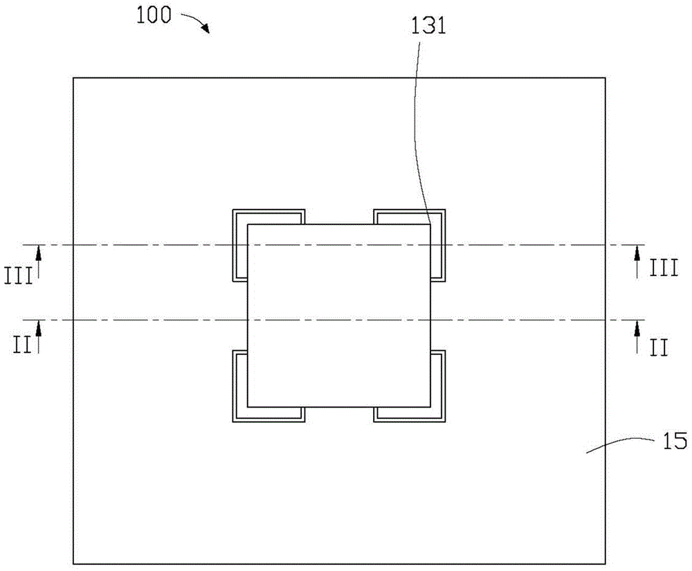
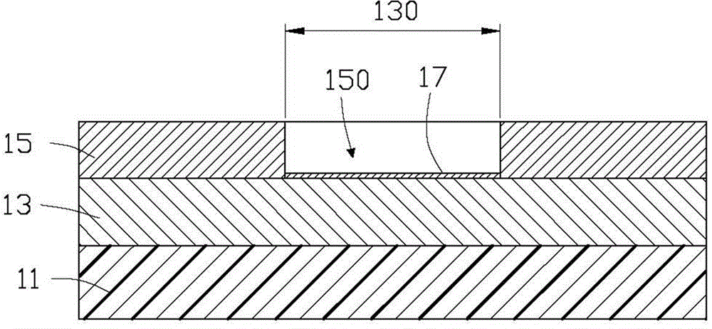
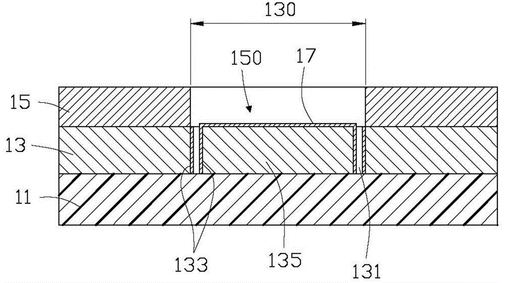
[0015] see Figure 1~Figure 2 , is a circuit board 100 provided in the first embodiment of the present invention. The circuit board 100 includes a substrate 11 , a conductive layer 13 , a solder resist layer 15 and a gold layer 17 .

[0016] The substrate 11 is used for supporting the conductive layer 13 , the solder resist layer 15 and the gold layer 17 . The base 11 is made of insulating material. The substrate 11 can be a polypropylene (PP) film, a polyester (PET) film or a polyimide (PI) film.

[0017] Please combine image 3 , the conductive layer 13 is located on the substrate 11 . The conductive layer 13 is copper foil. The conductive layer 13 has a conductive pattern to realize its electrical function. The conductive layer 13 includes a gold plating region 130 . The gold plating region 130 includes a connecting portion 135 ....


PUM


Abstract

The invention relates to a circuit board. The circuit board comprises a substrate, a conducting layer, a solder layer and a gold melting layer. The conducting layer is located on the substrate. The conducting layer comprises a gold melting area. The gold melting area comprises a connection portion. The solder layer covers the conducting layer, and the solder layer is provided with a window corresponding to the gold melting area. The conducting layer is provided with at least one opening in the gold melting area. Because of the at least one opening, the substrate is exposed. Each opening possesses a circumferential side wall. The circumferential side wall is a side surface of the conducting layer which is exposed by the opening. The gold melting layer is located in the gold melting area. The gold melting layer covers the connection portion and covers one circumferential side wall of each opening. The invention also relates to a manufacturing method of the circuit board.

Description

technical field [0001] The invention relates to a circuit board and a method for manufacturing the circuit board, in particular to a circuit board and a method for manufacturing the circuit board which can improve the phenomenon of gold jump plating. Background technique [0002] In the prior art, after the solder resist layer is formed on the copper clad laminate of the circuit board through a solder resist process, the solder resist layer usually exposes a part of the copper foil layer as a connection terminal (PAD) for connecting with an external electrical device. In order to prevent the exposed copper foil layer from being oxidized, a gold plating (electroless gold plating) process is subsequently performed on the exposed copper foil layer to form a gold plating layer on the exposed copper foil layer. However, at present, many products require the area of ​​the connecting terminal to be smaller and smaller, and the bubbles generated during the gold plating reaction are ...

Claims


Application Information

Patent Timeline
Patent Type & Authority Applications(China)
IPC IPC(8): H05K1/11H05K3/22H05K3/40
Inventor 向华李平
Owner AVARY HLDG (SHENZHEN) CO LTD
Why Eureka
Try Eureka