Band-gap reference voltage source with high power rejection ratio

A high power supply rejection ratio, reference voltage source technology, applied in the direction of adjusting electrical variables, control/regulating systems, instruments, etc., can solve the problems of complex structure, increased power consumption of bandgap reference voltage source, and higher manufacturing process requirements. Strong compatibility, improved power supply rejection ratio, and increased stability

Active Publication Date: 2016-03-09
SOUTHEAST UNIV
View PDF4 Cites 13 Cited by
  • Summary
  • Abstract
  • Description
  • Claims
  • Application Information

AI Technical Summary

Problems solved by technology

[0004] The traditional single bandgap reference voltage source suppresses the low-frequency noise signal mainly through the error amplifier in the circuit, and suppresses the high-frequency noise signal mainly through RC filtering. For the suppression of the intermed

Method used


Image

  • Band-gap reference voltage source with high power rejection ratio
  • Band-gap reference voltage source with high power rejection ratio
  • Band-gap reference voltage source with high power rejection ratio

Examples


Embodiment 1

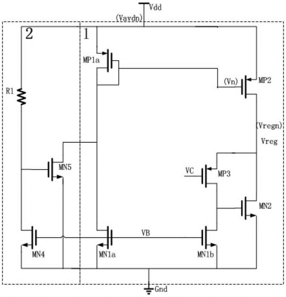
[0028] Embodiment 1: The circuit structures of the voltage self-regulating circuit 1 and the starting circuit 2 are as follows image 3 shown:

[0029] The voltage self-regulating circuit 1 includes PMOS transistors MP1a, MP2, MP3 and NMOS transistors MN1a, MN1b, MN2; wherein the sources of MP1a and MP2 are connected, and the connection point is connected to the DC power supply Vdd; the gate of MP1a is connected to the gate of MP2 At the same time, the gate of MP1a is connected to the drain, the drain of MP1a is connected to the drain of MN1a; the drain of MP2 is connected to the source of MP3, and the connection point is used as the first suppression signal output of the voltage self-regulating circuit 1 terminal, this connection point is connected to the drain of MN2 at the same time; the gate of MP3 is used as the second bias signal input terminal of the voltage self-regulating circuit 1, the drain of MP3 is connected to the gate of MN2 and is connected to the drain of MN1b...

Embodiment 2

[0059] Embodiment 2: According to the bandgap reference voltage source of Embodiment 1, the voltage self-regulating circuit 1 also includes a feedback circuit, and the feedback loop is as follows Figure 4 As shown, it includes: PMOS transistors MP1b, MP12 and NMOS transistors MN3a and MN3b; the sources of MP1b and MP12 are connected to the DC power supply Vdd, the gate of MP1b is connected to the gate of MP1a, and the drain of MP1b is connected to the drain of MN3a connected to the gate of MN3a; the gate of MN3a is connected to the gate of MN3b, the source of MN3a is connected to the source of MN3b and the connection point is connected to the drains of MP2 and MN2; the drain of MN3b is connected to the gate of MP2 at the same time It is connected to the gate and drain of MP12; where MP12 and MP3b form a feedback amplifier, MP1b and MN3a provide bias current for MN3b; the feedback loop controls the change of the output current of the voltage self-regulating circuit 1 within a c...


PUM


Abstract

The invention discloses a band-gap reference voltage source with the high power rejection ratio. The band-gap reference voltage source comprises a voltage self-adjustment circuit, a starting circuit, a first-order temperature compensation reference voltage generating circuit, an error amplifier, a bias voltage generating circuit and a reference starting circuit. According to the band-gap reference voltage source, power noise is inhibited to a certain degree through the voltage self-adjustment circuit, then power is supplied to a back-stage band-gap reference circuit, the noise is further inhibited through the band-gap reference circuit, and therefore the whole power source has the quite high power rejection ratio. In addition, the voltage self-adjustment circuit further comprises a feedback loop, an output current can be automatically adjusted, and the problem that as the current required by the back-stage circuit is increased suddenly, the whole circuit is unstable is solved; meanwhile, the power rejection ratio of the band-gap reference voltage source can be increased; compared with a traditional band-gap reference voltage source, stability is better, the power rejection ratio is higher, and the band-gap reference voltage source can meet high-accuracy working requirements.

Description

technical field [0001] The invention relates to a reference voltage source for radio frequency and digital-analog hybrid circuits, in particular to a bandgap reference voltage source with high power supply rejection ratio. Background technique [0002] With the rapid development of system integration technology, the reference voltage source has become an indispensable basic circuit module in digital and analog circuits, and is widely used in communication circuits, memory, sensors and other fields. The function of the reference voltage source is mainly to provide a stable reference voltage to other modules in the circuit. The stability of the reference voltage source is directly related to the working state of the circuit and the performance of the circuit. In order to meet the normal working requirements of the circuit in different external environments, the reference voltage source should have the advantages of stable output, strong anti-interference ability, and small tem...

Claims


Application Information

Patent Timeline
IPC IPC(8): G05F1/567
CPCG05F1/567G05F3/16
Inventor 吴建辉吴爱东林志伦杜媛姚芹李红陈超
Owner SOUTHEAST UNIV
Why Eureka
Try Eureka