Loop circuit compensating circuit used for Buck converter

A compensation circuit and converter technology, applied in the field of electronics, can solve the problems of reducing capacitor resistance area, large resistance and capacitance, difficult on-chip integration, etc., to reduce chip area and cost, small capacitance value, easy on-chip integration, etc. integrated effects

Inactive Publication Date: 2013-11-27
UNIV OF ELECTRONICS SCI & TECH OF CHINA
View PDF5 Cites 13 Cited by
  • Summary
  • Abstract
  • Description
  • Claims
  • Application Information

AI Technical Summary

Problems solved by technology

[0003] On-chip compensation can be divided into two types of compensation and three types of compensation. The second type of compensation is advanced phase compensation, which requires a small size of passive components and is suitable for on-chip integration. However, due to its low low-frequency gain, the steady-state error larger
The traditional three-type compensation is implemented by using an operational amplifier and a resistor-capacitor network. In order to obtain a low-frequency zero point, a large resistor and capacitor are required, which is difficult to integrate on-chip. Its structure is as follows: figure 1 shown
Literature (Patrick Y. Wu, Sam Y.S. Tsui and Philip K.T. Mok, "Area-and Power-Efficient Monolithic Buck Converters With Pseudo-Type III Compensation," IEEE Journal of Solid-State Circuits, vol.45, pp.1446–1455 ,Aug.2010.) A pseudo-three-type circuit structure was proposed, which reduced the capacitor resistance area and made on-chip integration possible, but the required on-chip capacitance value is 30pF, which is still too large for integrated circuits

Method used


Image

  • Loop circuit compensating circuit used for Buck converter
  • Loop circuit compensating circuit used for Buck converter
  • Loop circuit compensating circuit used for Buck converter

Examples


Embodiment Construction

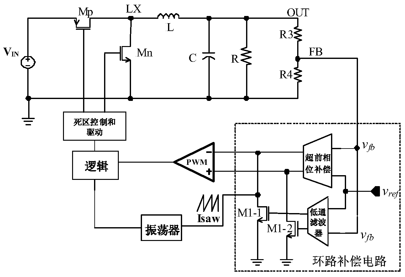
[0026] The principle of the loop compensation circuit of the present invention will be described below in conjunction with the accompanying drawings.

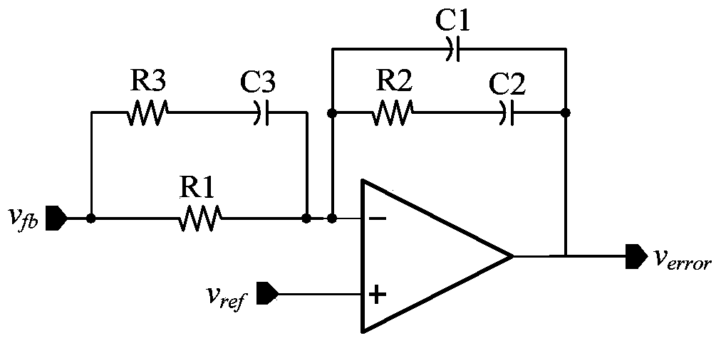
[0027] A loop compensation circuit for Buck converter, its structure is as follows figure 2 As shown, it includes an advanced phase compensation circuit, a fully differential low-pass filter and two NMOS transistors M1-1 and M1-2.

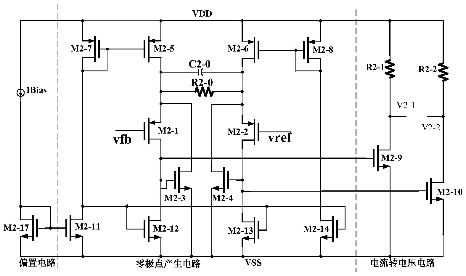
[0028] The lead phase compensation circuit, such as image 3 As shown, it consists of a first bias circuit, a pole-zero generating circuit and a current-to-voltage circuit. The lead phase compensation circuit generates a zero and two high frequency poles to provide lead phase compensation.

[0029] The first bias circuit is composed of a first current bias source IBias and an NMOS transistor M2-17; the first bias current source IBias is connected across the power supply VDD and the drain of the NMOS transistor M2-17, and the NMOS transistor M2- 17 The gate is short-circuited to the drain, and it...


PUM


Abstract

The invention discloses a loop circuit compensating circuit used for a Buck converter, and belongs to the technical field of electronics. The loop circuit compensating circuit used for the Buck converter comprises a leading phase compensating circuit and a full-differential low-pass filter circuit. The leading phase compensating circuit generates a zero point and two high-frequency poles to provide leading phase compensating; the full-differential low-pass filter circuit provides a pole and high lower-frequency gain; the output voltage of the leading phase compensating circuit and the output voltage of the full-differential low-pass filter circuit are added in a linear mode to acquire a voltage signal required by III-type compensating; because the high lower-frequency gain and two lower-frequency zero points are acquired, the defects that lower-frequency gain is low and steady-state errors are large in leading phase compensating are overcome. According to the loop circuit compensating circuit used for the Buck converter, because full-differential input and output structures are adopted in the leading phase compensating circuit and the low-pass filter circuit respectively, power supply rejection ratio (PSRR) is increased, the crosstalk problem among DC-DC converters in all paths of a PMU can be effectively solved.

Description

technical field [0001] The invention belongs to the field of electronic technology and relates to power supply technology, in particular to a loop compensation circuit for a step-down stabilized voltage converter (also known as a Buck converter). Background technique [0002] In recent years, with the rapid development of portable electronic products (such as mobile phones, tablet computers, MP3, etc.), the Power Management Unit (PMU) is increasingly valued and favored by people because of its high efficiency and adaptability to various load requirements. The PMU unit is composed of multiple DC-DC converters and control logic circuits. Among them, the Buck DC-DC converter is the core of the PMU unit, which is responsible for outputting the current and voltage required by the peripheral equipment. Buck converters can be divided into two types: off-chip compensation and on-chip compensation. Off-chip compensation requires additional PCB board area and off-chip compensation c...

Claims


Application Information

Patent Timeline
Patent Type & Authority Applications(China)
IPC IPC(8): H02M3/155H02M1/44
Inventor 甄少伟刘雨石王俊喜耿煜罗萍张波
Owner UNIV OF ELECTRONICS SCI & TECH OF CHINA
Why Eureka
Try Eureka