

Pixel circuit, driving method thereof, OLED display panel and display device
A pixel circuit and display panel technology, applied to static indicators, instruments, etc., can solve the problem of uneven display, achieve the effects of eliminating afterimages, prolonging life, and avoiding excessive charging time
- Summary
- Abstract
- Description
- Claims
- Application Information
AI Technical Summary
Problems solved by technology
Method used
Image

Examples
Embodiment 1
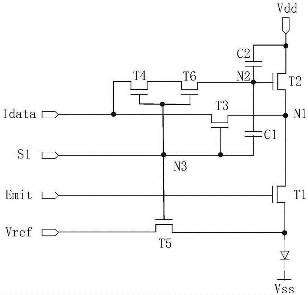
[0033] figure 1 A schematic structural diagram of a pixel circuit provided by Embodiment 1 of the present invention, as shown in figure 1 As shown, the present invention proposes a pixel circuit applied to an OLED display panel, including first to fourth transistors, first and second capacitors, and a light-emitting diode OLED, wherein the first electrode of the first transistor T1, the first The second electrode of the second transistor T2 and the second electrode of the third transistor T3 are connected to the first node N1, the gate of the second transistor T2, the second electrode of the fourth transistor T4 and one end of the first capacitor C1, the second One end of the second capacitor C2 is connected to the second node N2, the gates of the third transistor T3 and the fourth transistor T4 and the other end of the first capacitor C1 are connected to the third node N3; and
[0034] A first voltage signal S1 is input to the third node N3, a second voltage signal Emit is i...
Embodiment 2
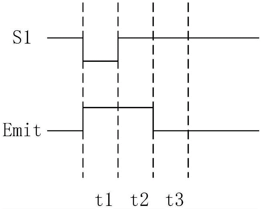
[0040] This embodiment provides a driving method for a pixel circuit, which is applied to the above-mentioned pixel circuit, and the driving method for the pixel circuit includes:
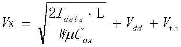
[0041] The first stage: the first voltage signal and the third voltage signal are low-level signals, the second voltage signal is a high-level signal, the second transistor is turned on, its threshold voltage and mobility are compensated, and the gate of the second transistor The voltage is charged to a certain voltage value Vx;
[0042] The second stage: the first voltage signal and the second voltage signal are high-level signals, and the third voltage signal is a low-level signal. Due to the coupling effect of the first capacitor, the gate voltage of the second transistor increases and becomes Vx+ Δx;
[0043] The third stage: the first voltage signal is a high-level signal, the second voltage signal and the third voltage signal are low-level signals, the first transistor is turned on, and the ...
Embodiment 3
[0052] This embodiment provides an OLED display panel, and the OLED display panel includes the pixel circuit described in the first embodiment.
[0053] The OLED display panel of this embodiment has the pixel circuit in the first embodiment, so by providing the data current signal and three voltage signals to the pixel circuit, the mixed compensation method of voltage driving and current driving is adopted, and at the same time, the threshold voltage of the driving transistor Compensated with the mobility, solved the problem of uneven display caused by it, and improved the display effect of the entire screen; since the first voltage signal changed from a low-level signal to a high-level signal in the second stage, the first The coupling of the capacitor increases the gate voltage of the second transistor, and the current flowing through the second transistor decreases in the second stage, which reduces the brightness in the third stage, so that when it is necessary to display a...
PUM
 Abstract
Description
Claims
Application Information