Check patentability & draft patents in minutes with Patsnap Eureka AI!

Method of improving low-dielectric film thickness stability

A technology with thin film thickness and low dielectric properties, which is applied in the manufacture of circuits, electrical components, semiconductors/solid-state devices, etc., can solve problems such as low film thickness, and achieve the effect of improving yield stability and improving stability

Active Publication Date: 2016-03-16
SHANGHAI HUALI MICROELECTRONICS CORP
View PDF5 Cites 0 Cited by
  • Summary
  • Abstract
  • Description
  • Claims
  • Application Information

AI Technical Summary

Problems solved by technology

[0005] Aiming at the defects such as low film thickness caused by the waiting time in the film forming process in the prior art, the present invention designs a method for improving the thickness stability of the low dielectric film, which improves the stability of the film

Method used


Image

  • Method of improving low-dielectric film thickness stability
  • Method of improving low-dielectric film thickness stability
  • Method of improving low-dielectric film thickness stability

Examples


Embodiment Construction

[0027] It should be noted that, in the case of no conflict, the following technical solutions and technical features can be combined with each other.

[0028] The specific embodiment of the present invention will be further described below in conjunction with accompanying drawing:

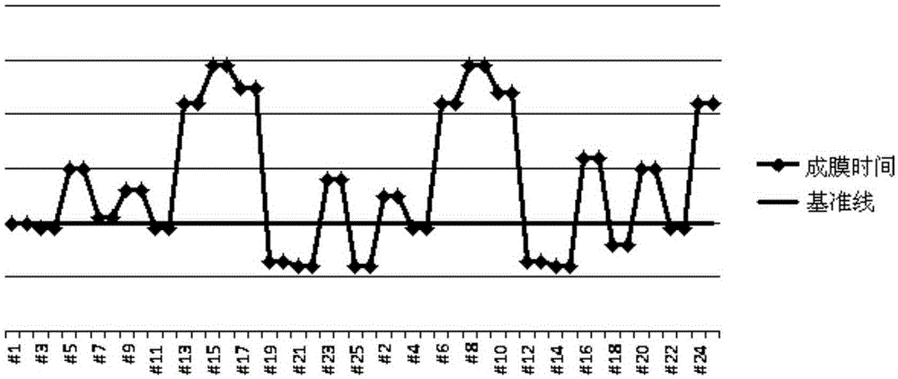
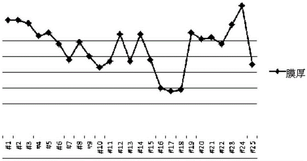
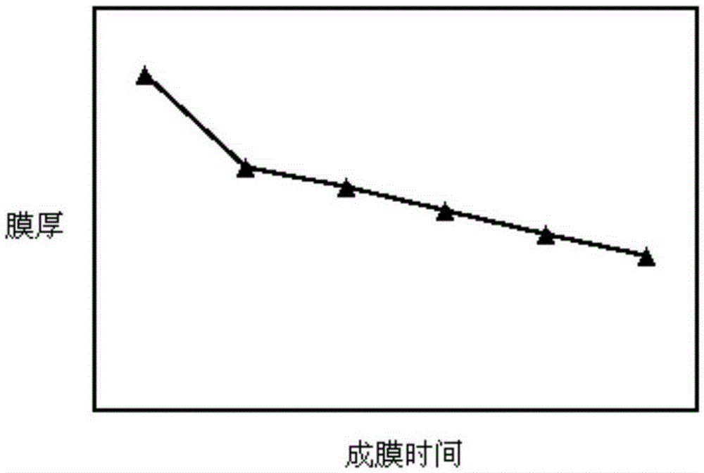
[0029] The invention mainly solves the problem of film thickness stability between transfers of low-kBD1 process silicon wafers in large-scale production. For the multi-silicon wafer film-forming process, when the wafer (wafer) is in continuous operation, the machine will enter a cycle. As the wafer process progresses, the hardware actions and process programs of the machine will be cycled. By collecting and analyzing the historical data of the operation, find out the cycle law of the film-forming pause time (completed film-forming time, idle time) and cleancount. For the wafers of the same cleancount, according to the idle time data (as long as the wafer continues to perform the process, the data...


PUM


Abstract

The invention relates to the field of semiconductors, and particularly relates to a method of improving low-dielectric film thickness stability. The method is applied to a formula for a multi-wafer film forming process. The method comprises steps: the average film forming time and the average film forming rate for each wafer group are collected; according to the collected average film forming time and the average film forming rate, the compensation time for each wafer group is calculated according to a calculation method; and the film forming time and the compensation time for a corresponding group are added to obtain the new film forming time for each group, and according to the new film forming time, the film forming process is carried out on the wafers.

Description

technical field [0001] The invention relates to the field of semiconductors, in particular to a method for improving the thickness stability of a low dielectric film. Background technique [0002] Low dielectric (Lowk) film is mainly used in the dielectric layer of the back section. Generally, octamethylcyclotetrasiloxane (OMCTS) and oxygen (O2) are used as the main reactants to form a film. OMCTS is formed under normal temperature and pressure. It is in a liquid state, and the film-forming reaction is very sensitive to temperature. After the reaction chamber (Processchamber) establishes the atmosphere, including Goclean, periodicclean, season, the longer the waiting time for the film formation process to start (processchamberidle), the less the amount of film formed on the surface of the wafer, and the film thickness on the wafer becomes thinner, among which , the relationship between the time to wait for the start of the film forming process and the film thickness is as f...

Claims


Application Information

Patent Timeline
IPC IPC(8): H01L21/31H01L21/02
CPCH01L21/02107H01L21/31
Inventor 钟飞沈剑平王科韩晓刚
Owner SHANGHAI HUALI MICROELECTRONICS CORP
Features
  • R&D
  • Intellectual Property
  • Life Sciences
  • Materials
  • Tech Scout
  • Unparalleled Data Quality
  • Higher Quality Content
  • 60% Fewer Hallucinations
Learn More