A kind of electrical packaging method of optoelectronic device

A technology of optoelectronic devices and packaging methods, which is applied in the field of optical communications, can solve the problems of reduced tolerance and difficulty in adding more PIN needles, and achieve the effects of reducing assembly difficulty, improving efficiency and reliability, and reducing production costs

Active Publication Date: 2017-05-31
HUBEI JIEXUN PHOTOELECTRIC
View PDF3 Cites 0 Cited by
  • Summary
  • Abstract
  • Description
  • Claims
  • Application Information

AI Technical Summary

Problems solved by technology

[0007] Design reasons, first of all, it is difficult to add more PIN pins at the bottom of traditional coaxial OSA devices, especially when the tolerance to other wiring in high-speed TO devices is greatly reduced

Method used


Image

  • A kind of electrical packaging method of optoelectronic device
  • A kind of electrical packaging method of optoelectronic device
  • A kind of electrical packaging method of optoelectronic device

Examples


Embodiment 1

[0027] Embodiment 1 takes a tunable optical receiving sub-module as an example to further describe the electrical packaging method of the optoelectronic device.

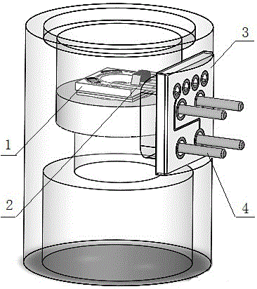
[0028] Such as image 3 As shown, a photoelectric device electrical packaging method, the optical device includes a housing, internal devices, the internal device includes an adjustable filter, a heating resistor 1 is attached to the adjustable filter; a plug is welded on the heating resistor 1 Needle or lead wire 2, ceramic substrate 3 is set on the side of the housing, the internal device is packaged by the combination of the housing and ceramic substrate 3, the ceramic substrate 3 is connected to the electrode of the internal device through the pin or lead wire 2, and the external pin is drawn out at the same time 4. The pins or leads 2 are fixed by welding or glue outside the package casing.

[0029] The pin or wire solution in this embodiment can be welded or glued outside the package shell, replacing the tradi...

Embodiment 2

[0033] Embodiment 2: as Figure 9 , Figure 10 Shown, the inventive method can also be used for photoelectric pulse tester, optical counter, comprise the photodiode with photoelectric switch; Or polarization detector, comprise full polarization state power detector, optical channel polarization state detector; Adjustable filter Partial replacement with switches or adjustable attenuators; any combination of adjustable filters, switches and adjustable attenuators, or a combination of all three; for specific two-port devices, electrical adjustment components, such as switches and attenuators, need to be added in the middle , Adjustable filter.

[0034] Figure 9 , Figure 10 Among them, 10-optical interface or mirror; 11-photoelectric switch, or electric adjustment components, such as micro-electromechanical switches, heating resistors, electric drive components, electro-optical modulators, etc., or electro-rotating polarizers, or shutter MEMS chips; 12 - Photodiode and elect...


PUM


Abstract

The invention belongs to the technical field of optical communication, and particularly relates to an electric packaging method for a photoelectric device. An optical device comprises a shell and an internal device, wherein a ceramic substrate is arranged on the side surface of the shell; the internal device is formed by combining and packaging the shell and the ceramic substrate; the ceramic substrate is connected with an electrode of the internal device through a thrusting needle or a lead, and simultaneously external pins are led out; and the thrusting needle or the lead is welded or fixed with glue outside the packaged shell. The electric packaging method solves the design problem that the lead needs to be manufactured on the side surface of the device after the integration level of a sealed long axis-shaped or long strip-shaped packaging device is gradually improved, packaging and lead requirements are carried out in a limited space range for specific requirements of micro device modules, and modularized mass production can be met, so that the production efficiency is greatly improved, and the production cost is reduced; and according to the electric packaging method, the assembly difficulty is greatly reduced, and the efficiency and reliability are improved.

Description

technical field [0001] The invention belongs to the technical field of optical communication, and in particular relates to an electrical packaging method for an optoelectronic device. Background technique [0002] With the trend of more and more compact device structure and higher integration and complexity, the original method of stacking multiple devices is gradually replaced by an integrated mini-package structure. [0003] This trend includes a phenomenon: the original coaxial device or two-stage, three-stage and multi-stage devices, such as coaxial packaged devices used in large quantities, because more electronic control components need to be included The circuit interface or leads, and such devices often have fixed leads or electrical interfaces on the top and bottom, so this type of integrated device needs to be connected to the electrical leads from the side. [0004] For example figure 1 , figure 2 As shown, there are circuit connections or other connections su...

Claims


Application Information

Patent Timeline
Patent Type & Authority Patents(China)
IPC IPC(8): H01L31/18
CPCH01L31/18Y02P70/50
Inventor 卢卫东聂媛杨昕黎凯
Owner HUBEI JIEXUN PHOTOELECTRIC
Why Eureka
Try Eureka