Manufacturing method of one-sided double-contact flexible circuit board

A flexible circuit board, single-sided and double-contact technology, which is used in the manufacture of printed circuits, the formation of printed circuits, and the formation of electrical connection of printed components. Copper surface damage and other problems, to achieve the effect of saving production cost and production time

Inactive Publication Date: 2016-03-23
SHENZHEN SUNTAK MULTILAYER PCB
View PDF5 Cites 4 Cited by
  • Summary
  • Abstract
  • Description
  • Claims
  • Application Information

AI Technical Summary

Problems solved by technology

This method has the following disadvantages: when laser drilling is used to make reverse pads, the energy uniformity is difficult to control, and residual glue on the pad surface or copper surface damage is prone to occur. Moreover, the production time and cost of opening windows by laser drilling are relatively high

Method used


Image

  • Manufacturing method of one-sided double-contact flexible circuit board
  • Manufacturing method of one-sided double-contact flexible circuit board
  • Manufacturing method of one-sided double-contact flexible circuit board

Examples


Embodiment

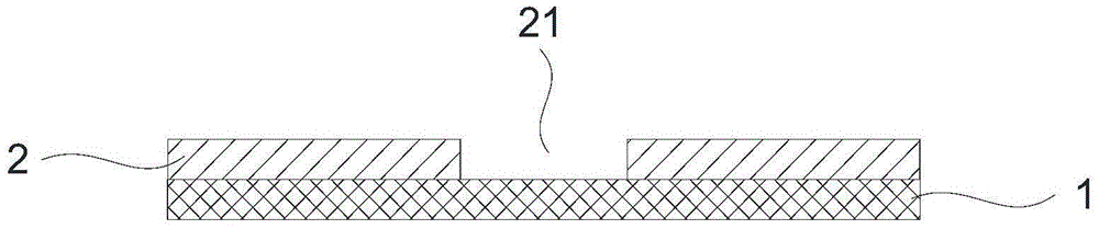
[0018] Such as figure 1 As shown, a front cover film window 21 is provided at the position corresponding to the pad to be exposed on the front cover film 2 , and the front cover film window 21 is 0.15mm smaller than a single side of the required pad. Then the front cover film 2 and the pure copper foil 1 are pressed together.

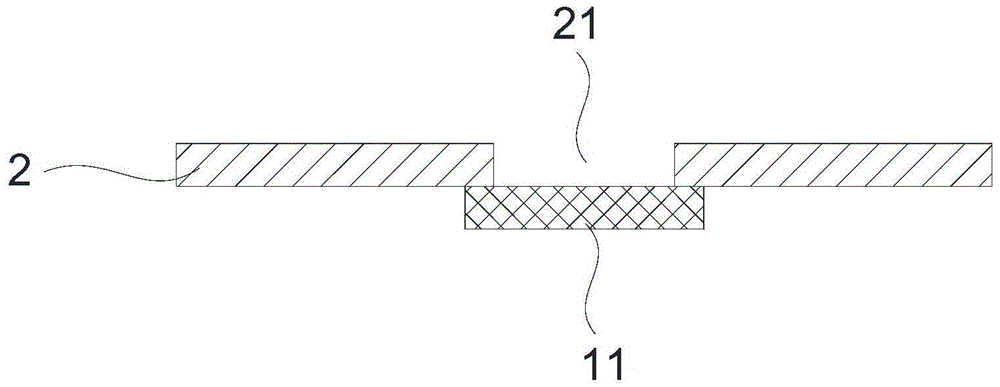
[0019] Such as figure 2 As shown, the pure copper foil 1 is etched to form a copper circuit by making a circuit pattern, and the pure copper foil corresponding to the position of the window 21 of the front cover film of the copper circuit is reserved to form a pad 11 .

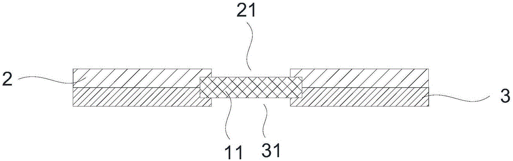
[0020] Such as image 3 As shown, a back cover film window 31 is provided at the position corresponding to the pad 11 to be exposed on the back cover film 3 , and the back cover film window 31 is 0.1 mm smaller than a single side of the required pad 11 . The back cover film 3 is pressed on the side of the copper circuit opposite to the front cover film 21, and the position of the w...


PUM


Abstract

The present invention discloses a manufacturing method of a one-sided double-contact flexible circuit board, and relates to the technical field of circuit board production. The manufacturing method comprises the following steps: S1, press-fitting a front side cover film provided with a window on a surface of pure copper foil; S2, by making a circuit pattern, etching the pure copper foil to form a copper circuit, wherein the pure copper foil, at a position corresponding to the window in step S1, of the copper circuit is kept, to form a pad; and S3, press-fitting a back side cover film provided with a window on a side, opposite to the front side cover film, of the pure copper foil, wherein a position of the window of the back side surface cover film corresponds to a position of the pad in the step S2. According to the manufacturing method of the one-sided double-contact flexible circuit board provided by the present invention; the cover films are press-fit on two sides of the pure copper foil; the windows are disposed in the cover films before the cover films are press-fit; and the cover films on the two sides are press-fit respectively before and after the circuit pattern is made. Copper surface adhesive residue and copper surface damage caused by using a laser to make a window on a back side pad in the existing method are avoided. Moreover, the process of using a laser to make a window on the back side of the pad is eliminated, thereby significantly reducing the manufacturing cost and the manufacturing time.

Description

technical field [0001] The invention relates to the technical field of circuit board production, in particular to a method for manufacturing a single-sided double-contact flexible circuit board. Background technique [0002] In single-sided flexible circuit boards, due to product assembly requirements, some pads have soldering requirements on both sides. This type of circuit board is called "single-sided double-contact" flexible circuit board. It is made as Figure 4 As shown, a single-sided copper-clad laminate substrate 6 is used, and after the circuit board pattern is made, the cover film 4 that has been windowed (windowed part 41) is pressed to expose the front side of the pad 5, and then the laser drilling method is used to Burn through the PI base material (laser processing part 61 ) on the back of the circuit board to expose the back side of the pad 5 . This method has the following disadvantages: when laser drilling is used to make reverse pads, it is difficult to c...

Claims


Application Information

Patent Timeline
Patent Type & Authority Applications(China)
IPC IPC(8): H05K3/00H05K3/40
CPCH05K3/0064H05K3/40H05K2203/0323
Inventor 宇超彭卫红何淼
Owner SHENZHEN SUNTAK MULTILAYER PCB
Why Eureka
Try Eureka