mos transistor and method of making the same

A technology of MOS transistors and manufacturing methods, which is applied in the field of MOS transistors and their manufacture, can solve the problems of slow carrier mobility of MOS transistors, and achieve the effect of improving carrier mobility and fast carrier mobility

Active Publication Date: 2018-09-07
SEMICON MFG INT (SHANGHAI) CORP
View PDF3 Cites 0 Cited by
  • Summary
  • Abstract
  • Description
  • Claims
  • Application Information

AI Technical Summary

Problems solved by technology

[0006] The technical problem to be solved by the present invention is to improve the problem that the carrier mobility rate of the MOS transistor is too slow

Method used


Image

  • mos transistor and method of making the same
  • mos transistor and method of making the same
  • mos transistor and method of making the same

Examples


Embodiment Construction

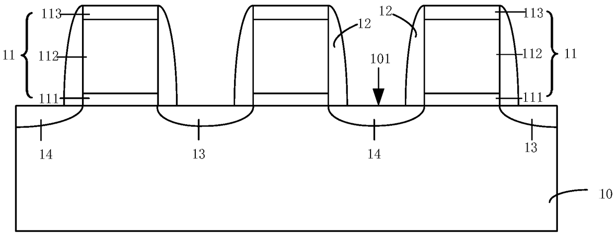
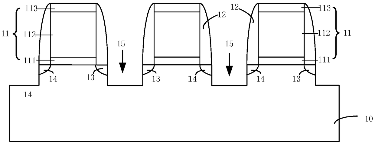
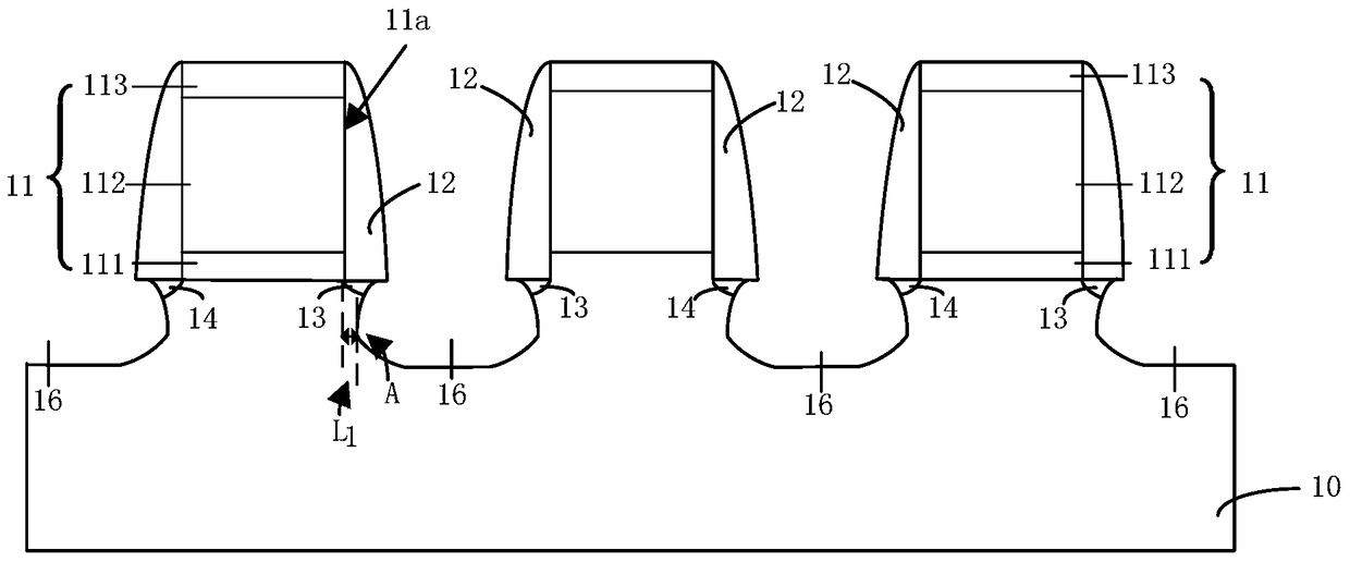
[0044] As mentioned in the background technology, the carrier mobility rate of existing embedded MOS transistors is still relatively slow. To solve the above problems, the present invention increases the amount of compressive stress material or tensile stress material filled in the source and drain regions. , thereby increasing the tensile or compressive stress applied to the channel. Specifically, by enlarging the size of the opening of the bowl-shaped groove that is scheduled to form the source and drain regions to make it larger than the distance between adjacent side walls, the size of the opening of the sigma-shaped groove formed thereafter is also larger .

[0045] In order to make the above objects, features and advantages of the present invention more comprehensible, specific embodiments of the present invention will be described in detail below in conjunction with the accompanying drawings.

[0046] Figure 1 to Figure 4 is a cross-sectional view of a PMOS transistor d...


PUM


Abstract

The invention discloses a MOS transistor and a manufacturing method therefor. In order to improve the carrier migration rate of the MOS transistor, the size of an opening of a bowl-shaped groove is controlled during the forming of a sigma-shaped groove, so as to enable the size of the opening to be greater than the distance between side walls of the adjacent grid structures. In other words, the size of the opening of the bowl-shaped groove is controlled to be great as much as possible, thereby enabling the size of the opening of the sigma-shaped groove formed by the corrosion of the bowl-shaped groove to be greater, enabling pressure stress materials or tensile stress materials placed in a source-drain region to be more, enabling the tensile stress or pressure stress applied to a trench to be greater, and enabling the carrier migration rate to be greater.

Description

technical field [0001] The invention relates to the field of semiconductor manufacturing, in particular to a MOS transistor and a manufacturing method thereof. Background technique [0002] With the improvement of integrated circuit integration, the size of semiconductor devices is gradually scaled down. In the process of scaling down the size of semiconductor devices, the drain voltage does not decrease accordingly, which leads to the gap between the source and drain. The electric field in the track area increases, and under the action of a strong electric field, electrons will accelerate to a speed many times higher than the speed of thermal motion between two collisions. Because the kinetic energy of electrons is very large, the electrons are called hot electrons, which cause hot electrons Effect (hot electron effect). The hot electron effect will cause hot electrons to be injected into the gate dielectric layer, forming gate electrode current and substrate current, thus...

Claims


Application Information

Patent Timeline
Patent Type & Authority Patents(China)
IPC IPC(8): H01L29/78H01L21/336
Inventor 刘佳磊
Owner SEMICON MFG INT (SHANGHAI) CORP
Why Eureka
Try Eureka