Band gap voltage source circuit

A sub-bandgap, voltage source technology, applied in the direction of adjusting electrical variables, control/regulation systems, instruments, etc., can solve the problems of current consumption, large occupation, large chip area, etc., to reduce current power consumption and chip area Effect

Active Publication Date: 2016-04-06
WUXI ZGMICRO ELECTRONICS CO LTD
View PDF5 Cites 0 Cited by
  • Summary
  • Abstract
  • Description
  • Claims
  • Application Information

AI Technical Summary

Problems solved by technology

so, figure 1 Each module needs to consume the corr

Method used


Image

  • Band gap voltage source circuit
  • Band gap voltage source circuit

Examples


Example Embodiment

[0021] In order to make the above objectives, features and advantages of the present invention more obvious and understandable, the present invention will be further described in detail below with reference to the accompanying drawings and specific embodiments.

[0022] The "one embodiment" or "embodiment" referred to herein refers to a specific feature, structure, or characteristic that can be included in at least one implementation of the present invention. The appearances of "in one embodiment" in different places in this specification do not all refer to the same embodiment, nor are they separate or selectively mutually exclusive embodiments with other embodiments. Unless otherwise specified, the words connected, connected, and connected in this text indicating electrical connection all mean direct or indirect electrical connection.

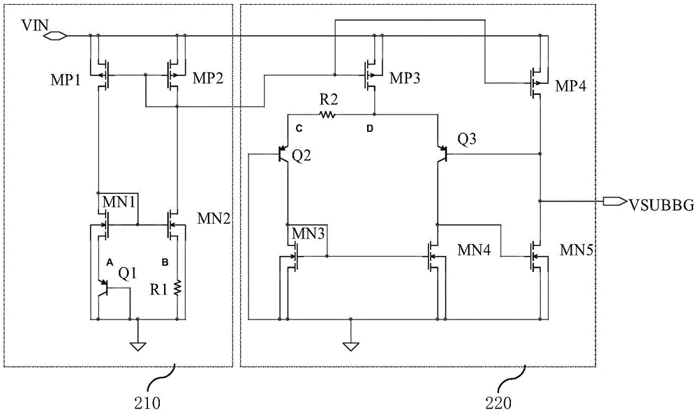
[0023] Please refer to figure 2 As shown, it is a circuit diagram of the sub-bandgap voltage source circuit in one embodiment of the present in...


PUM


Abstract

The invention provides a band gap voltage source circuit comprising a bias circuit and a band gap voltage generation circuit. The bias circuit outputs bias voltage; the band gap voltage generation circuit has MOS pipes (MP3, MP4,MN3,MN4 and MN5), bipolar transistors Q2 and Q3 and resistance R2; source electrodes of the MP3 and MP4 are connected with a power supply end; grids of the MOS pipes are connected with an output end of the bias circuit; a drain electrode of the MP4 is connected with a drain electrode of the MN5; a drain electrode of the MP3 is connected with an emitter of the Q2 via the resistance R2; a grid of the Q2 is grounded and a collector electrode of the Q2 is connected with a drain electrode of MN3; an emitter of the Q3 is connected with the drain electrode of the MP3 and a collector electrode of the Q3 is connected with a drain electrode of the MN4; a grid of the MN4 is connected with a grid of the MN3; source electrodes of the MN3, MN4 and MN5 are grounded; a grid of the MN5 is connected with the drain electrode of the MN4; a connection node between the MP4 and MN5 is connected with a base electrode of the Q3; and the connection node works as an output end of the band gap voltage to be connected. Compared with the prior art, power consumption of a chip can be reduced and area of the chip can be reduced.

Description

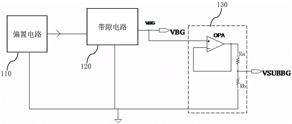
【Technical field】 [0001] The invention relates to the technical field of reference voltages, in particular to a sub-bandgap voltage source circuit. 【Background technique】 [0002] Please refer to figure 1 As shown, it is a schematic circuit diagram of a sub-bandgap voltage source circuit in the prior art, which includes a bias circuit 110 , a bandgap circuit 120 and a voltage divider circuit 130 . Wherein, the bias circuit 110 generates a current bias to provide a bias current for the bandgap circuit 120; the bandgap circuit 120 generally generates a bandgap voltage VBG of about 1.25V, which is determined by the energy bandgap of the semiconductor; the voltage divider circuit 130 includes Operational amplifier OPA, voltage divider resistors Ra and Rb, the specific connection relationship is as follows figure 1 As shown, the operational amplifier OPA provides the current for driving the resistors Ra and Rb. In addition, the operational amplifier OPA is isolated between the ...

Claims


Application Information

Patent Timeline
IPC IPC(8): G05F3/22
Inventor 王钊
Owner WUXI ZGMICRO ELECTRONICS CO LTD
Why Eureka
Try Eureka