Curved-face liquid crystal panel

A technology for liquid crystal panels and curved surfaces, applied in nonlinear optics, instruments, optics, etc., can solve the problems of image distortion, pixel area mismatch, and increased panel energy consumption on curved liquid crystal panels, avoiding fringe field coupling capacitance, Avoid light leakage and reduce the effect of brightness

Inactive Publication Date: 2016-04-13
NANJING CEC PANDA LCD TECH
View PDF5 Cites 7 Cited by
  • Summary
  • Abstract
  • Description
  • Claims
  • Application Information

AI Technical Summary

Problems solved by technology

The CF substrate 300 takes its center as the base point, its left side slides to the left relative to the TFT substrate 100, and its right side slides to the right relative to the TFT substrate 100, so that the black matrix 301 no longer corresponds to the data line 101, but instead The radial direction of the curved liquid crystal panel is misaligned, which leads to the mismatch between the pixel area of ​​the TFT substrate 100 and the CF substrate, and defects such as light leakage and crosstalk, resulting in distortion of the displayed image of the curved liquid crystal panel and a decrease in optical quality.
[0005] In order to avoid light leakage caused by BM misalignment when the display is bent, the prior art uses an enlarged width of the common electrode 102 on the TFT substrate as a light-shielding layer such as image 3 As shown, but this will cause the coupling capacitance between the common electrode 102 and the data line 101 to increase, which will increase the energy consumption of the panel

Method used


Image

  • Curved-face liquid crystal panel
  • Curved-face liquid crystal panel
  • Curved-face liquid crystal panel

Examples


Embodiment Construction

[0019] Below in conjunction with accompanying drawing and specific embodiment, further illustrate the present invention, it should be understood that these embodiments are only used to illustrate the present invention and are not intended to limit the scope of the present invention, after having read the present invention, those skilled in the art understand various aspects of the present invention Modifications in equivalent forms all fall within the scope defined by the appended claims of this application.

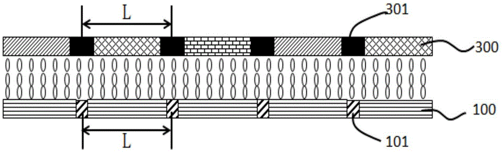
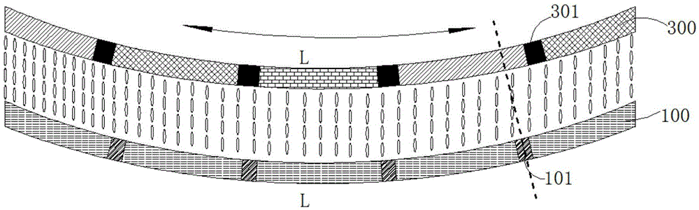
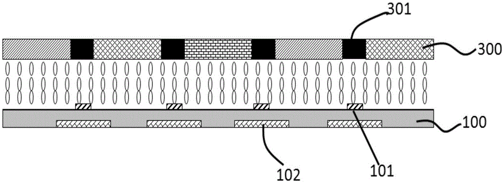
[0020] In order to overcome the problems of the prior art, the present invention provides a curved liquid crystal panel, such as Figure 4-5 As shown, the panel includes a TFT substrate 200, a CF substrate 300 disposed corresponding to the TFT substrate, and a liquid crystal layer 400 disposed between the TFT substrate and the CF substrate. The CF substrate 300 includes a filter area 302 and a black matrix 301, wherein the width N of the black matrix 301 is 3-6um; the fi...


PUM


Abstract

The invention discloses a curved-face liquid crystal panel which comprises a TFT substrate, a CF substrate corresponding to the TFT substrate and a liquid crystal layer arranged between the TFT substrate and the CF substrate. The CF substrate comprises a filter area and a black matrix. The TFT substrate comprises a plurality of data lines, common electrodes and pixel electrodes. The common electrodes comprise the first common electrode, the second common electrode and a common electrode connecting line for connecting the first common electrode with the second common electrode, the first common electrode, the second common electrode and the common electrode connecting line are of an H-shaped structure, and the first common electrode and the second common electrode are partially overlapped with the data line. The first common electrode and the second common electrode are overlapped with the pixel electrodes adjacent to the first and second common electrodes respectively. According to the technical scheme, when the panel is in a curved face state, light leakage caused by black matrix dislocation is avoided, the brightness will not be lowered, the aperture opening ratio is improved, and energy consumption is reduced.

Description

technical field [0001] The invention belongs to the field of liquid crystal display devices, in particular to a curved liquid crystal panel. Background technique [0002] Large size, light and thin, high resolution and high quality picture are the development trend of display at present. Ordinary large-size VA displays have technical limitations such as narrow viewing angles, color shift, and distortion. In order to break through the current technical drawbacks, curved displays have emerged as the times require. Curved liquid crystal displays are gradually favored for their wider viewing angles, reduced distortion for close-up viewing, and product differentiation. [0003] The curved LCD panel is the core component of the curved LCD. The existing manufacturing process of the curved liquid crystal panel is as follows: first, the flat liquid crystal panel is manufactured, and then the flat liquid crystal panel is bent to form the curved liquid crystal panel. Such as figure...

Claims


Application Information

Patent Timeline
Patent Type & Authority Applications(China)
IPC IPC(8): G02F1/1343G02F1/1362
CPCG02F1/134309G02F1/136213G02F2201/121
Inventor 王杰刘文雄
Owner NANJING CEC PANDA LCD TECH
Why Eureka
Try Eureka