Transistor forming method

A technology of transistors and dummy gates, which is applied in the field of semiconductor manufacturing, can solve the problems of reduced device density, difficulty in controlling the process of high-K metal gate transistors, and unstable performance of high-K metal gate transistors, etc., and achieves the effect of reducing the difficulty of the process

Active Publication Date: 2016-04-20
SEMICON MFG INT (SHANGHAI) CORP
View PDF3 Cites 7 Cited by
  • Summary
  • Abstract
  • Description
  • Claims
  • Application Information

AI Technical Summary

Problems solved by technology

[0005] However, with the continuous reduction of semiconductor process nodes, the size of the formed high-k metal gate transistors is continuously reduced and the device density is con...

Method used


Image

  • Transistor forming method
  • Transistor forming method
  • Transistor forming method

Examples


Embodiment Construction

[0034] As mentioned in the background art, with the shrinking of semiconductor process nodes, the process difficulty of forming high-k metal gate transistors increases, and the formed high-k metal gate transistors have poor performance.

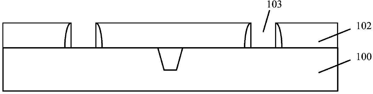
[0035] The forming process of the high-K metal gate transistor is a gate last (GateLast) process, Figure 1 to Figure 4 It is a schematic cross-sectional structure diagram of the formation process of a high-K metal gate transistor according to an embodiment of the present invention.

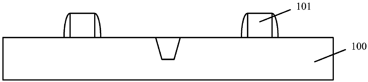
[0036] Please refer to figure 1 A substrate 100 is provided, the surface of the substrate 100 has a dummy gate layer 101, the material of the dummy gate layer 101 is polysilicon, and the dummy gate layer 101 occupies a space and a position for a subsequently formed metal gate.

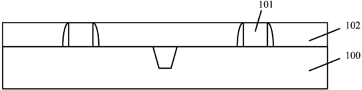
[0037] Please refer to figure 2 , forming a dielectric layer 102 on the surface of the substrate 100 , the dielectric layer 102 covers the sidewall of the dummy gate layer 101 , and t...


PUM

PropertyMeasurementUnit
Thicknessaaaaaaaaaa
Thicknessaaaaaaaaaa
Thicknessaaaaaaaaaa

Abstract

The invention discloses a transistor forming method. The transistor forming method is characterized in that a dummy grid film is disposed on a surface of a substrate; the dummy grid film is provided with ions in a doped manner, and a doped area and a non-doped area are formed in the dummy grid film, and in addition, the surface of the doped area is aligned with the surface of the dummy grid film, and the non-doped area is disposed on the bottom part of the doped area; after the dummy grid film is provided with the ions in a doped manner, parts of the dummy grid film can be etched until parts of the surface of the substrate is exposed, and the surface of the substrate is provided with dummy grid layers; the side walls of the dummy grid layers can be thinned, and the side walls of the non-doped area is recessed with respect to the side walls of the doped area; after the thinning of the side walls of the dummy grid layers, source-drain areas can be formed in the substrate on two sides of the dummy grid layers; after the forming of the source-drain areas, and dielectric layers can be formed on the surface of the substrate, and in addition, the dielectric layers are disposed on the side walls of the dummy grid layers in a covered manner, and the surfaces of the dielectric layers are aligned with the surfaces of the dummy grid layers; the dummy grid layers are removed, and first openings are formed in the dielectric layers; and grids can be formed in the first openings. The performance of the formed transistor can be improved.

Description

technical field [0001] The invention relates to the technical field of semiconductor manufacturing, in particular to a method for forming a transistor. Background technique [0002] With the rapid development of integrated circuit manufacturing technology, the size of semiconductor devices in integrated circuits, especially MOS (Metal Oxide Semiconductor, metal-oxide-semiconductor) devices, is continuously reduced to meet the miniaturization and integration of integrated circuit development. Requirements, and transistor devices are one of the important components of MOS devices. [0003] For transistor devices, as the size of the transistor continues to shrink, the gate dielectric layer formed of silicon oxide or silicon oxynitride material in the prior art cannot meet the performance requirements of the transistor. In particular, transistors formed with silicon oxide or silicon oxynitride as the gate dielectric layer are prone to a series of problems such as leakage curren...

Claims


Application Information

Patent Timeline
IPC IPC(8): H01L21/336
Inventor 赵杰
Owner SEMICON MFG INT (SHANGHAI) CORP
Why Eureka
Try Eureka