Semiconductor light emitting element

A technology for light-emitting elements and semiconductors, applied in semiconductor devices, electrical components, circuits, etc., can solve problems such as low luminous efficiency and achieve the effect of improving light extraction efficiency

Inactive Publication Date: 2016-04-20
USHIO DENKI KK
View PDF5 Cites 0 Cited by
  • Summary
  • Abstract
  • Description
  • Claims
  • Application Information

AI Technical Summary

Problems solved by technology

At this time, most of the current flows in the light-emitting layer directly under the n-side electrode, and almost no current flows in the other light-emitting layers, so there is a problem that the light-emitting area is limited and the luminous efficiency is low.

Method used


Image

  • Semiconductor light emitting element
  • Semiconductor light emitting element
  • Semiconductor light emitting element

Examples


no. 1 Embodiment approach

[0059] The structure of the first embodiment of the semiconductor light emitting element of the present invention will be described.

[0060] structure

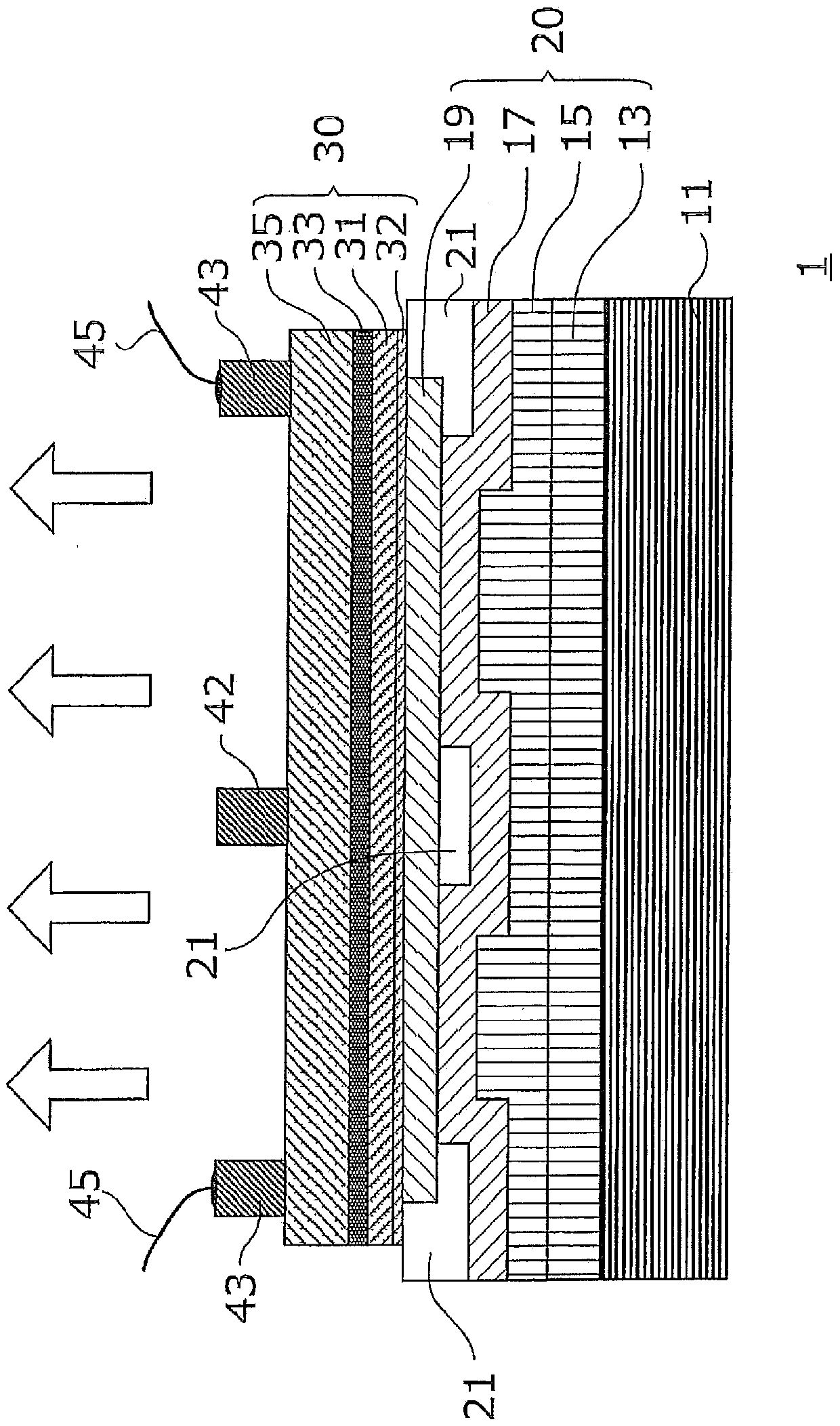
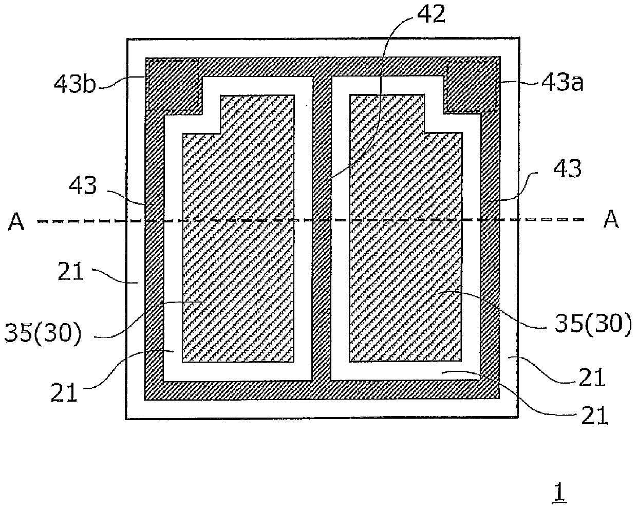
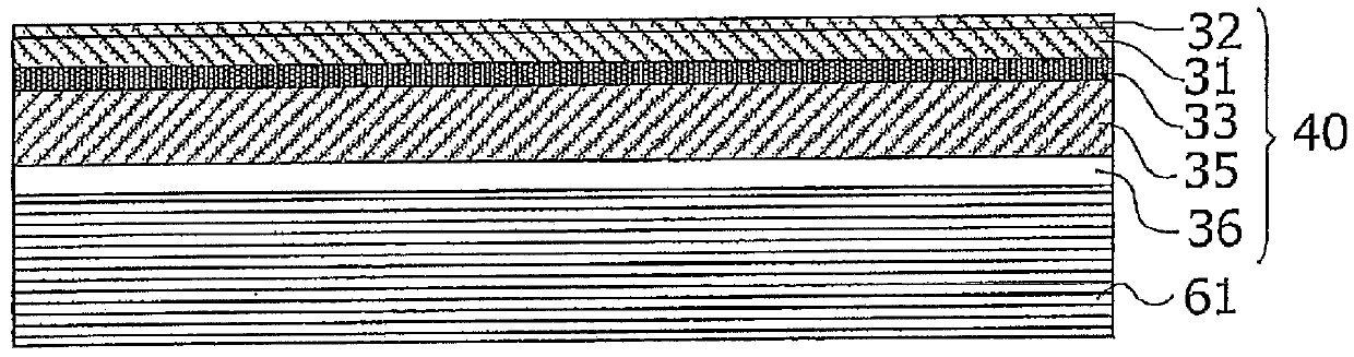
[0061] Figure 1A It is a cross-sectional view schematically showing the structure of the semiconductor light emitting element of the first embodiment. The semiconductor light emitting element 1 is configured to include a support substrate 11, a conductive layer 20, an insulating layer 21, a semiconductor layer 30, and n-side electrodes (42, 43). The semiconductor layer 30 is formed by stacking a p-type semiconductor layer ( 32 , 31 ), a light emitting layer 33 , and an n-type semiconductor layer 35 sequentially from below. in addition, Figure 1B It is a schematic plan view when viewing the semiconductor light emitting element 1 from above, Figure 1A and Figure 1B Corresponds to the A-A line sectional view in.

[0062] (Support substrate 11)

[0063] The supporting substrate 11 is formed of, for example, a conductiv...

no. 2 Embodiment approach

[0135] The structure of the second embodiment of the semiconductor light emitting element of the present invention will be described. In addition, the same code|symbol is attached|subjected to the same structure as 1st Embodiment, and description is abbreviate|omitted.

[0136]

[0137] image 3 It is a cross-sectional view schematically showing the structure of the semiconductor light emitting element of the second embodiment. Compared with the semiconductor light emitting element 1 of the first embodiment, the semiconductor light emitting element 1 a further includes an insulating layer 22 (corresponding to "the second insulating layer"). The insulating layer 22 is also made of SiO 2 , SiN, Zr 2 o 3 , AlN, Al 2 o 3 And so on.

[0138] More specifically, the insulating layer 22 is formed at a position directly under the formation position of the n-side electrodes ( 42 , 43 ) and sandwiched between the reflective electrode 19 and the p-type semiconductor layer 32 . F...

Embodiment

[0151] The semiconductor light emitting element 1 of the first embodiment manufactured by the method described above is referred to as Example 1, the semiconductor light emitting element 1a of the second embodiment is referred to as Example 2, and Figure 5 The semiconductor light-emitting element 50 shown is used as a comparative example, and the current-voltage characteristics and light-emitting characteristics are compared.

[0152] Figure 5It is a cross-sectional view schematically showing the structure of a semiconductor light emitting element formed as a comparative example. Compared with the semiconductor light emitting element 1 , the insulating layer 23 provided on the upper surface of the reflective electrode 19 is provided instead of the insulating layer 21 formed on the bottom surface of the reflective electrode 19 . The insulating layer 23 is formed for the purpose of spreading the current flowing in the light emitting layer 33 in the horizontal direction by bei...


PUM

PropertyMeasurementUnit
Thicknessaaaaaaaaaa
Thicknessaaaaaaaaaa
Thicknessaaaaaaaaaa

Abstract

Provided is a semiconductor light emitting element wherein light extraction efficiency is further improved, while ensuring spreading of a current flowing in a light emitting layer, said spreading being in the horizontal direction. This semiconductor light emitting element is configured such that the semiconductor light emitting element has, on a supporting substrate, an n-type semiconductor layer, a p-type semiconductor layer, and a light emitting layer that is formed between the n-type semiconductor layer and the p-type semiconductor layer. The semiconductor light emitting element is provided with: an n-side electrode that is formed by having the bottom surface thereof in contact with the upper surface of the n-type semiconductor layer; a reflection electrode, which has the upper surface thereof in contact with the bottom surface of the p-type semiconductor layer, and which is formed in a region including a position just below the area where the n-side electrode is formed; and a first insulating layer, which is formed by having the upper surface thereof in contact with the bottom surface of the reflection electrode, said first insulating layer being formed at a position just below the area where the n-side electrode is formed.

Description

technical field [0001] The present invention relates to a semiconductor light-emitting element having an n-type semiconductor layer, a p-type semiconductor layer, and a light-emitting layer formed therebetween on a support substrate. Background technique [0002] Conventionally, GaN has been mainly used in light-emitting devices using nitride semiconductors. At this time, from the viewpoint of lattice matching, a GaN film with few defects is formed by epitaxial growth on a sapphire substrate, thereby forming a light-emitting element made of a nitride semiconductor. Here, since the sapphire substrate is an insulating material, when power is supplied to the GaN-based light-emitting element, a part of the p-type semiconductor layer is removed to expose the n-type semiconductor layer, and each of the p-type semiconductor layer and the n-type semiconductor layer is exposed. An electrode for power supply is formed on the semiconductor layer. In this way, a light-emitting element...

Claims


Application Information

Patent Timeline
IPC IPC(8): H01L33/38H01L33/32
CPCH01L33/405H01L33/38
Inventor 杉山彻月原政志三好晃平南部纱织
Owner USHIO DENKI KK
Why Eureka
Try Eureka