Pixel unit, infrared imaging detector provided with pixel unit and manufacturing process

A pixel unit and infrared imaging technology, which is applied in the field of infrared detection, can solve problems such as difficult cost reduction, poor reliability, and complicated preparation process, and achieve the effects of small thermal mass, improved fill factor, and simple preparation process

Active Publication Date: 2016-04-27
HUAZHONG UNIV OF SCI & TECH
View PDF6 Cites 10 Cited by
  • Summary
  • Abstract
  • Description
  • Claims
  • Application Information

AI Technical Summary

Problems solved by technology

However, the preparation process of this improved structure is complicated, the reliability is poor, and the cost is difficult to reduce

Method used


Image

  • Pixel unit, infrared imaging detector provided with pixel unit and manufacturing process
  • Pixel unit, infrared imaging detector provided with pixel unit and manufacturing process
  • Pixel unit, infrared imaging detector provided with pixel unit and manufacturing process

Examples


Embodiment Construction

[0029] The specific embodiments of the present invention will be further described below in conjunction with the accompanying drawings. It should be noted here that the descriptions of these embodiments are used to help understand the present invention, but are not intended to limit the present invention. In addition, the technical features involved in the various embodiments of the present invention described below can be combined with each other as long as they do not constitute a conflict with each other.

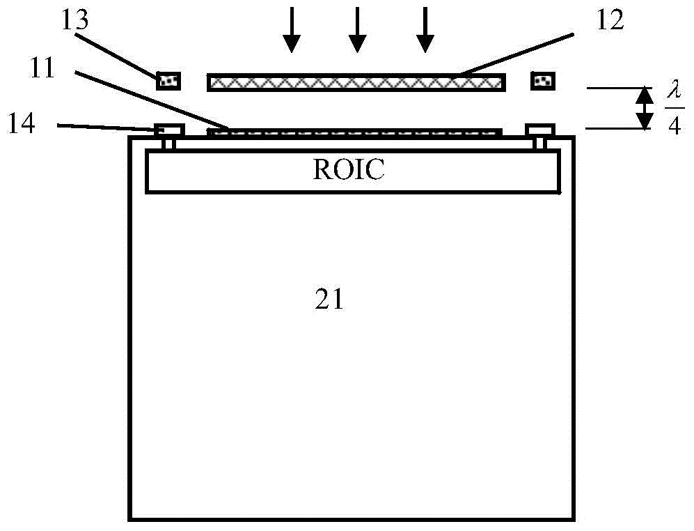
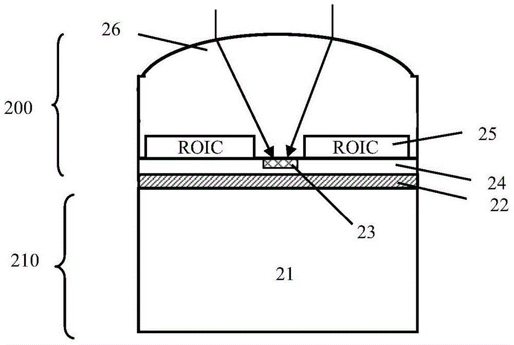
[0030] figure 2 It is a vertical cross-sectional view of a single pixel of an infrared detector. The pixel is mainly formed by bonding a thin silicon-based active sheet 200 and a passive support sheet 210. Therefore, the pixel unit structure after bonding from bottom to top includes: a support layer 21, a bonding layer 22, and a photosensitive unit. 23. A dielectric layer 24, a readout circuit (ROIC) layer 25, and a silicon microlens layer 26.

[0031] The material o...


PUM


Abstract

The invention discloses an uncooled infrared detection pixel unit with a nanostructure photosensitive unit and adopting a backlighting mode and a planar array infrared imaging detector chip formed by the pixel unit. The detector chip is formed by bonding a silicon-based active sheet with a photosensitive unit array and a passive substrate sheet playing a supporting role. A large amount of two-dimensional arrays formed by the pixel units are arranged on the active sheet, and each pixel unit is composed of a central infrared transmission channel on the front surface of the silicon substrate, an ROIC readout circuit on the periphery of the transmission channel, a nanostructure photosensitive unit in the pixel center, a surface dielectric layer and a focused micro optic unit on the back surface of the silicon substrate. The infrared light is incident from one side of a micro lens on the back surface of the silicon substrate, the light is converged by the micro lens and is then focused on the nanostructure photosensitive unit on the front surface of the silicon substrate via the light transmission channel to be absorbed and detected. The backlighting nanostructure infrared detector has the advantages of high fill factors and quick response, the device structure and the manufacturing process are simple, and the backlighting nanostructure infrared detector can be used for manufacturing a low-cost infrared thermal imager.

Description

technical field [0001] The invention belongs to the technical field of infrared detection, and relates to a backlighting infrared detection pixel unit with a nanostructure photosensitive element, an uncooled infrared imaging detector composed of the pixel unit and a preparation process thereof. Background technique [0002] The current uncooled infrared imaging detectors based on the principle of microbolometers all adopt the front-illuminated heat-sensitive film absorption detection method. figure 1 Pixel vertical cross-section for a microbolometer detector operating in the previous illumination regime. The infrared absorbing layer 12 containing the photosensitive film is suspended on the surface of the silicon substrate 21 containing the readout circuit (ROIC) through the supporting bridge legs 13 on both sides. The surface of the supporting legs 13 also contains conductive electrodes so that the two ends of the photosensitive unit are respectively connected to the ROIC. ...

Claims


Application Information

Patent Timeline
Patent Type & Authority Applications(China)
IPC IPC(8): G01J5/20H01L27/146
Inventor 赖建军李宏伟黄鹰
Owner HUAZHONG UNIV OF SCI & TECH
Why Eureka
Try Eureka