Wafer back thinning method

A backside thinning and wafer technology, applied in electrical components, semiconductor/solid-state device manufacturing, circuits, etc., can solve problems such as silicon material waste

Inactive Publication Date: 2016-05-04
SHANGHAI HUALI MICROELECTRONICS CORP
View PDF3 Cites 3 Cited by
  • Summary
  • Abstract
  • Description
  • Claims
  • Application Information

AI Technical Summary

Problems solved by technology

All of the above methods can achieve the thinning of the backside of the wafer, but it

Method used


Image

  • Wafer back thinning method

Examples


Embodiment Construction

[0028] In order to make the content of the present invention clearer and easier to understand, the content of the present invention will be described in detail below in conjunction with specific embodiments and accompanying drawings.

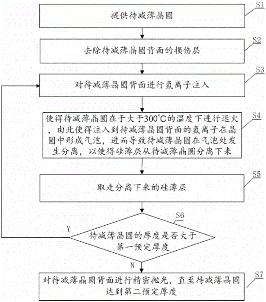
[0029] The invention proposes a method for thinning the back of the wafer. After removing the damaged layer on the back of the wafer, the silicon on the back of the wafer is peeled off layer by layer by using hydrogen ion implantation and high-temperature annealing process, thereby realizing wafer back thinning. At the same time, the stripped silicon thin layer can be further utilized, such as making solar cells.

[0030] figure 1 A flow chart of a wafer backside thinning method according to a preferred embodiment of the present invention is schematically shown.

[0031] Such as figure 1 As shown, the wafer backside thinning method according to a preferred embodiment of the present invention includes:

[0032] The first step S1: provide the w...


PUM

PropertyMeasurementUnit
Thicknessaaaaaaaaaa
Diameteraaaaaaaaaa
Thicknessaaaaaaaaaa

Abstract

The invention provides a wafer back thinning method, comprising a first step of providing a to-be-thinned wafer; a second step of removing the damaged layer on the back of the to-be-thinned wafer; a third step of injecting hydrogen ions on the back of the to-be-thinned wafer; a fourth step of annealing the to-be-thinned wafer at a temperature of more than 300 degrees centigrade, enabling the hydrogen ions injected on the back of the to-be-thinned wafer to form bubbles in the wafer, further causing the to-be-thinned wafer to separate in the bubbles, thus separating thin silicon layers from the to-be-thinned wafer; a fifth step of taking away the separated thin silicon layers; and a sixth step of judging whether the thickness of the to-be-thinned wafer is more than a first preset thickness, if the thickness of the to-be-thinned wafer is more than the first preset thickness, repeating the third to fifth steps to the rest to-be-thinned wafer.

Description

technical field [0001] The invention relates to the field of semiconductor manufacturing, and more specifically, the invention relates to a wafer back thinning method. Background technique [0002] The technological progress of IC is changing with each passing day, and it is developing in the direction of high speed, high integration, high density and high performance. With the continuous improvement of integration, speed and reliability, microelectronic products are developing in the direction of thinner, lighter and smaller. In line with this, new chip packaging technologies are constantly emerging, and the chip thickness required by these advanced packaging technologies is getting thinner and thinner. . The thickness of silicon wafers with a diameter of 150mm and 200mm are 625um and 725um respectively, while the average thickness of silicon wafers with a diameter of 300mm will reach 775um. The effective thickness of the circuit layer on the silicon wafer is generally 5-...

Claims


Application Information

Patent Timeline
IPC IPC(8): H01L21/02H01L21/265H01L21/324
CPCH01L21/02H01L21/265H01L21/3247
Inventor 雷通
Owner SHANGHAI HUALI MICROELECTRONICS CORP
Why Eureka
Try Eureka