Global pixel nonlinear compensation structure

A non-linear compensation and global pixel technology, which is applied in electrical components, image communication, television, etc., can solve the problem of the circuit dynamic range becoming smaller, and achieve the effects of improving dynamic range, optimizing timing, and reducing power consumption

Active Publication Date: 2016-05-04
SHANGHAI INTEGRATED CIRCUIT RES & DEV CENT +1
View PDF8 Cites 3 Cited by
  • Summary
  • Abstract
  • Description
  • Claims
  • Application Information

AI Technical Summary

Problems solved by technology

[0048] The nonlinearity introduced in the whole circuit is undesirable, and the nonlinearity here makes the actual Tc smaller, and the final effect is that the dynamic range of the circuit is smaller

Method used


Image

  • Global pixel nonlinear compensation structure
  • Global pixel nonlinear compensation structure
  • Global pixel nonlinear compensation structure

Examples


Embodiment Construction

[0073] The specific embodiment of the present invention will be further described in detail below in conjunction with the accompanying drawings.

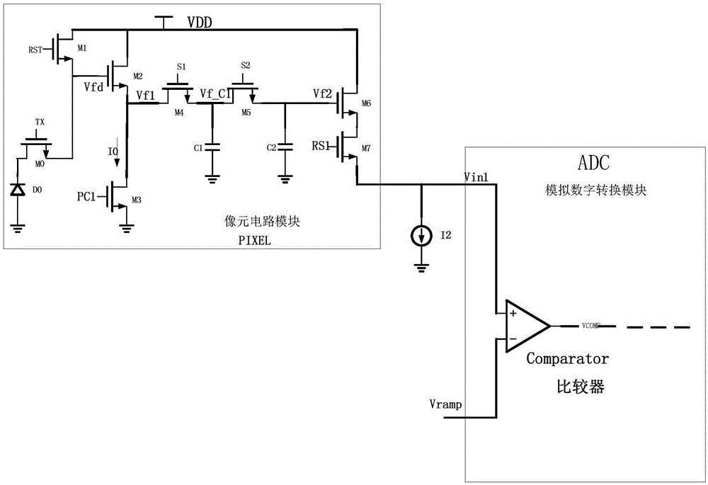
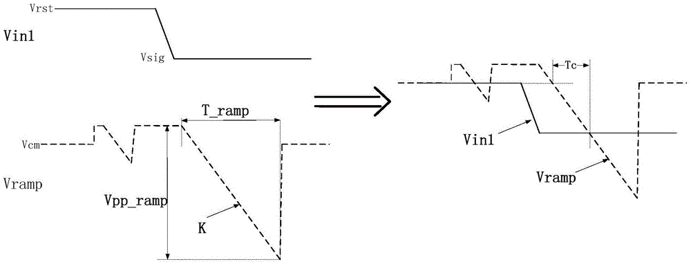
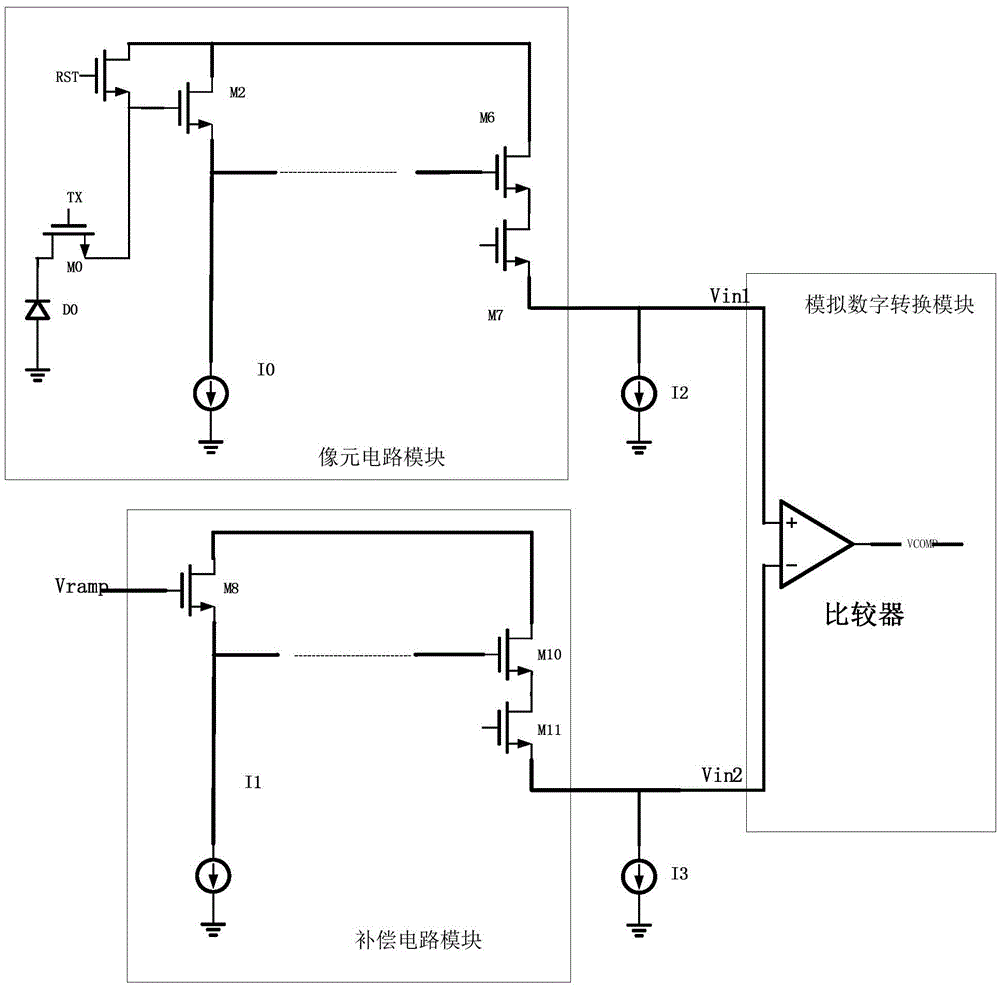
[0074] see image 3 , image 3 Shown is a schematic diagram of the global pixel nonlinear compensation structure proposed by the present invention. As shown in the figure, the circuit shown in the upper frame on the left can be a pixel circuit module; the analog-digital conversion module shown on the right includes a positive input terminal Vin1 and a pixel The circuit module is connected and its negative input terminal Vin2 receives the comparator of the reference voltage Vramp; the circuit shown in the upper box on the left side is a new compensation circuit module in the embodiment of the present invention, and the compensation circuit module is connected between the reference voltage Vramp signal and The negative input terminal Vin2 of the comparator is used to compensate the non-linearity introduced by the internal circuit of...


PUM


Abstract

The invention provides a global pixel nonlinear compensation structure. A global pixel includes a pixel circuit module and an analog-to-digital conversion module; the analog-to-digital conversion module comprises a comparator which is provided with a positive input end Vin1 connected with the pixel circuit module and a negative input end Vin2 receiving reference voltage Vramp; the nonlinear compensation structure comprises a compensation circuit module; and the compensation circuit module is connected between reference voltage Vramp signals and the negative input end Vin2 of the comparator and is used for compensating nonlinearity led by the inner circuit of the pixel circuit module. With the global pixel nonlinear compensation structure of the invention adopted, the nonlinearity of the global pixel can be compensated, and the dynamic range of the global pixel can be improved; and a time sequence can be optimized when the nonlinearity is compensated; and power consumption which is as low as possible is just brought.

Description

technical field [0001] The present invention relates to the field of integrated circuit technology, in particular to the field of CMOS image sensors, and more specifically, to a global pixel nonlinear compensation method, that is, a global pixel nonlinear compensation structure. Background technique [0002] An image sensor is a sensor chip that can convert optical signals reflecting image information into electrical signals, and is divided into two categories: CCD structure and CMOS structure. In today's image sensor market, CMOS image sensors are widely used due to their advantages of low cost, high speed, low power consumption, continuously improving image quality, and compatibility with CMOS processes. [0003] A CMOS image sensor is a typical solid-state imaging sensor. A CMOS image sensor is usually composed of an image sensor array, a row driver, a column driver, a timing control logic, an AD converter, a data bus output interface, and a control interface. The above-...

Claims


Application Information

Patent Timeline
IPC IPC(8): H04N5/374H04N5/3745
CPCH04N25/77H04N25/76
Inventor 何学红董林妹张远
Owner SHANGHAI INTEGRATED CIRCUIT RES & DEV CENT
Why Eureka
Try Eureka