Chip automatic detection method

An automatic detection and chip detection technology, which is applied in the direction of measuring devices, optical testing of flaws/defects, and material analysis through optical means, can solve the problems of large chip pollution, large manual intervention, and low efficiency, and reduce unfavorable factors. Realize the effect of automation and high detection efficiency

Inactive Publication Date: 2016-05-11
上海恒浥智能科技股份有限公司
View PDF8 Cites 8 Cited by
  • Summary
  • Abstract
  • Description
  • Claims
  • Application Information

AI Technical Summary

Problems solved by technology

In the existing operation process, this series of actions are all done manually, and individual steps are realized through automatic operation, but generally speaking, manual intervention is large, efficiency is low, and pollution to the chip is large

Method used


Image

  • Chip automatic detection method
  • Chip automatic detection method
  • Chip automatic detection method

Examples


Embodiment Construction

[0038] The specific implementation of the chip automatic detection method of the present invention will be described in detail below with reference to the accompanying drawings.

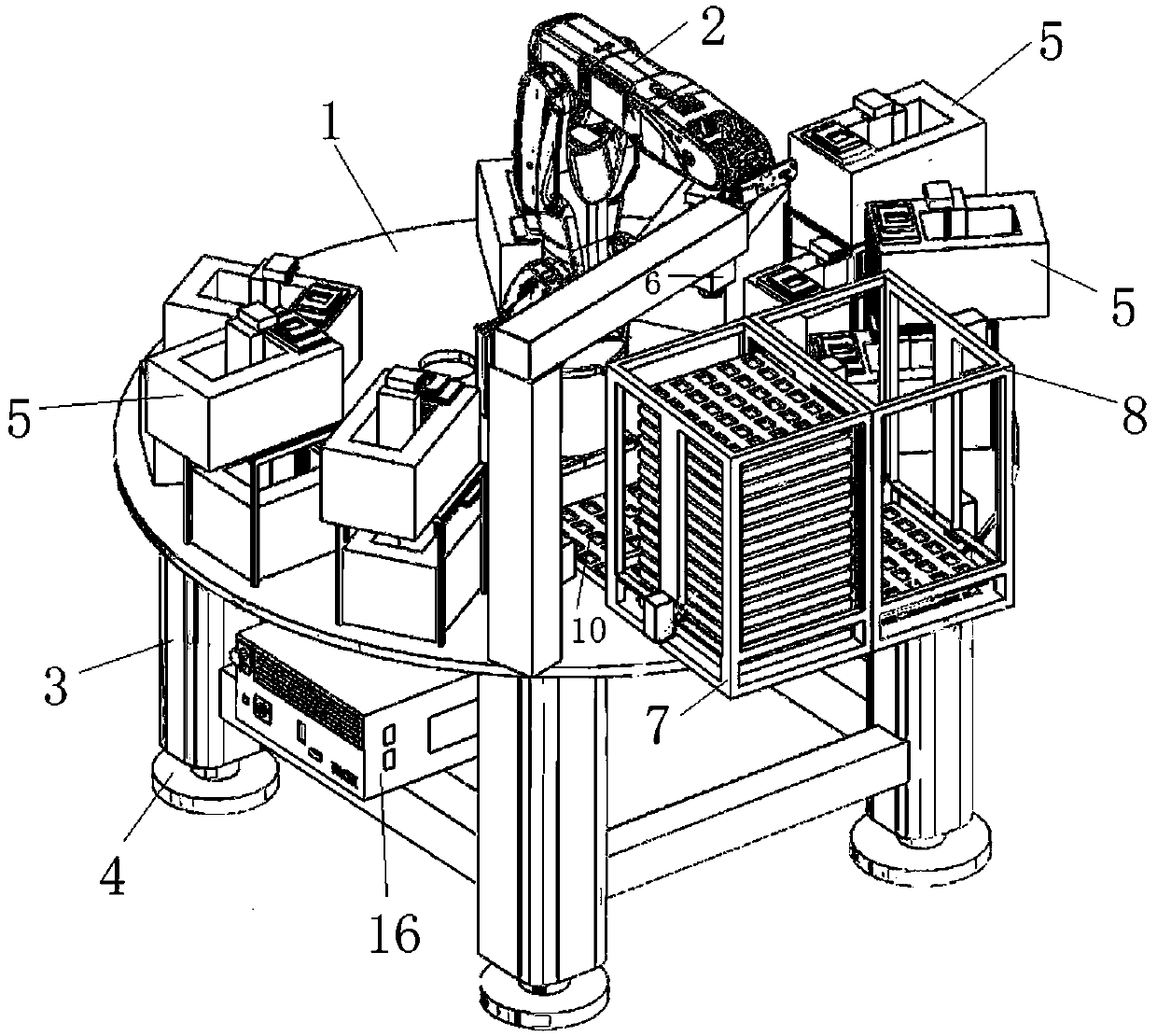
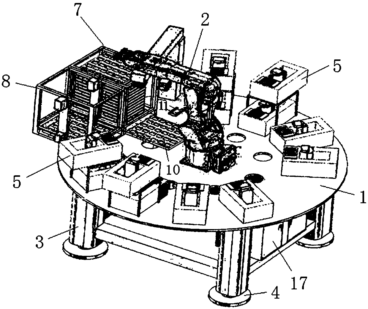
[0039] See attached figure 1 , 2 The automatic chip detection device includes a workbench 1, a robot 2 arranged in the middle of the workbench 1, a control module, and the like. The workbench 1 is circular, the workbench 1 is supported by four supporting feet 3, a crosspiece is arranged between the supporting feet 3, and a roller 4 is arranged on the supporting feet 3.

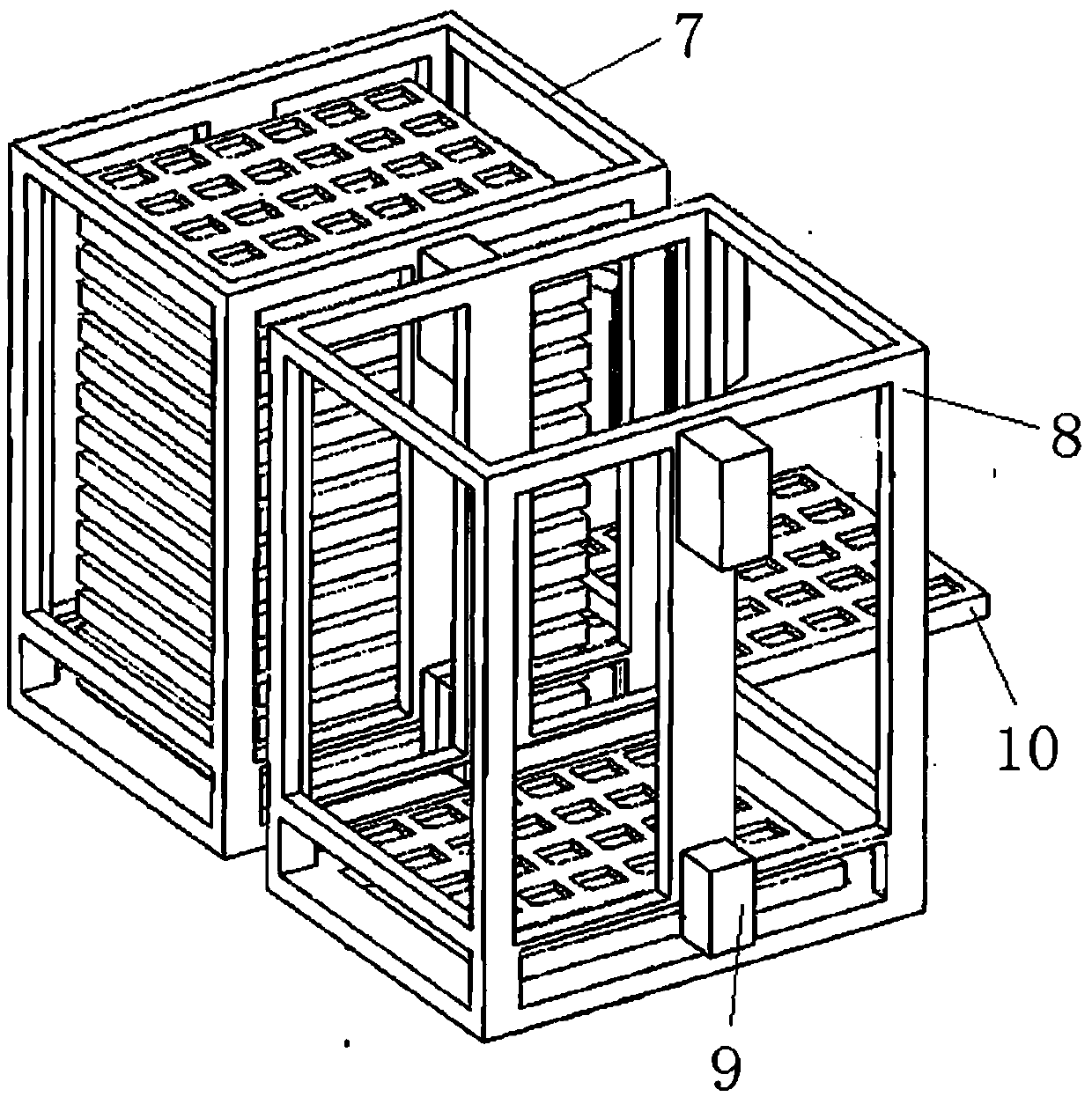
[0040] A storage bin and a plurality of chip detection boxes 5 are respectively arranged around the workbench 1, and the chip detection boxes 5 are arranged on the workbench 1 in a circular array. A vision camera 6 is provided on the side of the silo through a camera bracket. The silo includes an upper silo 7 and a lower silo 8, and the upper silo 7 and the lower silo 8 are arranged side by side.

[0041] See attached image 3 , The silo i...


PUM


Abstract

The invention belongs to the technical field of integrated circuit chip production, processing, and detection, and discloses a chip automatic detection method. The method comprises the following steps: loading material discs into a feeding chamber, delivering the material discs to a feeding station, taking pictures of the material discs and sending the chip position by a visual camera, sending a feeding signal by a chip detection box, catching the chips in the material disc by a robot, catching the chips that have been detected by a suction disc claw, placing the chips into a chip detection box by the suction disc claw to detect the chips, delivering the detected chips to a material disc or a waste material box, delivering the material disc that has been detected to a discharge chamber, and detecting all material discs in the feeding chamber. The method has the advantages that the chip detection becomes automatic, the detection efficiency is high, and the unfavorable factors brought by artificial intervention are reduced.

Description

Technical field [0001] The invention belongs to the technical field of integrated circuit chip production and processing detection, in particular to a chip automatic detection method. Background technique [0002] After the finished integrated circuit chip is produced, the chip must be inspected. The inspection content includes physical defect inspection, magnetic induction inspection, etc. After inspection, qualified chips must be packaged, and unqualified chips must be recycled. In the existing operation process, these series of actions are completed manually, and individual steps are realized through automated operations. However, in general, manual intervention is large, the efficiency is low, and the chip pollution is large. Summary of the invention [0003] In order to solve the above technical problems, the present invention provides an automatic chip detection method, which realizes rapid chip detection through a fully automated process. [0004] The technical scheme adopte...

Claims


Application Information

Patent Timeline
Patent Type & Authority Applications(China)
IPC IPC(8): G01N21/95B07C5/342
CPCB07C5/342G01N21/9501
Inventor 任宁
Owner 上海恒浥智能科技股份有限公司
Why Eureka
Try Eureka