Method for forming semiconductor structure

A semiconductor and gate structure technology, applied in the field of semiconductor structure formation, to achieve the effects of good shape, stable and easy-to-control stress, and accurate size

Active Publication Date: 2016-05-11
SEMICON MFG INT (SHANGHAI) CORP
View PDF2 Cites 5 Cited by
  • Summary
  • Abstract
  • Description
  • Claims
  • Application Information

AI Technical Summary

Problems solved by technology

[0004] However, the stress layer formed in the source and drain regions of the transistor by the existing process can no longer

Method used


Image

  • Method for forming semiconductor structure
  • Method for forming semiconductor structure
  • Method for forming semiconductor structure

Examples


Embodiment Construction

[0035]As mentioned in the background art, the stress provided by the stress layer formed in the source region and the drain region of the transistor cannot meet the technical requirements, and the stress on the channel region of the transistor needs to be further increased.

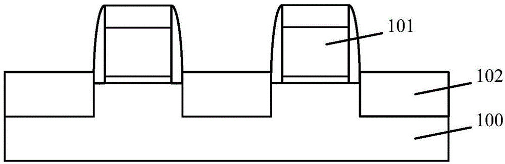
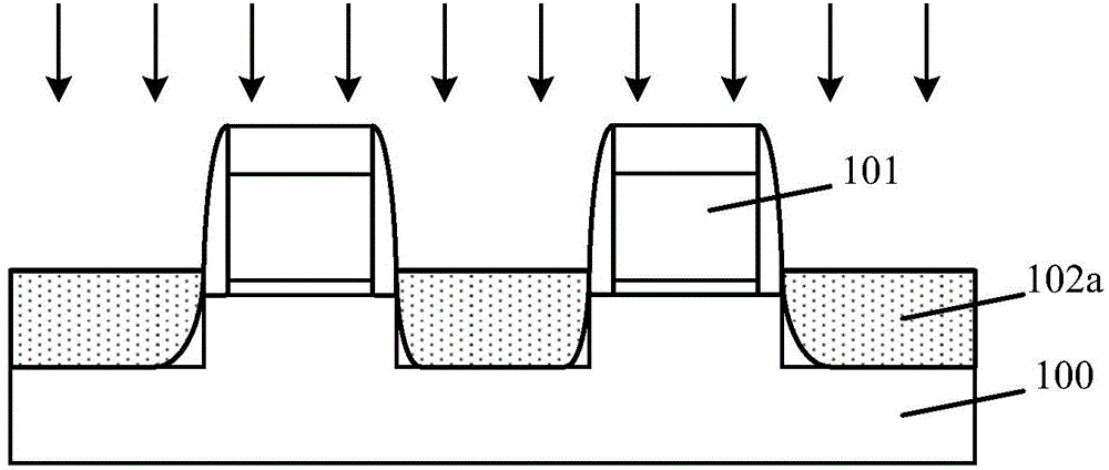
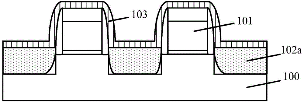
[0036] Please refer to figure 1 , figure 1 It is a schematic cross-sectional structure diagram of a transistor with a source region and a drain region with a stress layer according to an embodiment of the present invention, including: a substrate 100; a gate structure 101 located on the surface of the substrate 100; and a substrate 100 located on both sides of the gate structure 101 Inner stress layer 102 .

[0037] Since the embedded stress layer (embedded stress layer) is formed behind the source and drain regions of the transistor, the stress layer can apply stress to the substrate due to the lattice mismatch between the stress layer and the substrate, and the stress layer is inserted into the subst...


PUM

PropertyMeasurementUnit
Thicknessaaaaaaaaaa

Abstract

A method for forming a semiconductor structure comprises the following steps: providing a substrate; forming gate structures on the surface of the substrate; forming an initial stress layer on the surface of the substrate on the two sides of the gate structures, wherein the material of the initial stress layer is amorphous; forming a cover stress layer on the surface of the initial stress layer; and after the cover stress layer is formed, converting the material of the initial stress layer into a crystalline material through a solid-phase process, and forming a source and drain stress layer. The morphology and the performance of the formed semiconductor structure are improved.

Description

technical field [0001] The invention relates to the technical field of semiconductor manufacturing, in particular to a method for forming a semiconductor structure. Background technique [0002] With the rapid development of semiconductor manufacturing technology, semiconductor devices are developing towards higher component density and higher integration. Transistors are currently being widely used as the most basic semiconductor devices, so as the component density and integration of semiconductor devices increase, the gate size of transistors becomes smaller than before (. However, the smaller gate size of transistors will Make transistor produce short channel effect, and then produce leakage current, finally affect the electrical performance of semiconductor device.At present, prior art mainly improves semiconductor device performance by improving carrier mobility.When the mobility of carrier improves, transistor If the driving current is increased, the leakage current ...

Claims


Application Information

Patent Timeline
IPC IPC(8): H01L21/336H01L29/78
Inventor 洪中山
Owner SEMICON MFG INT (SHANGHAI) CORP
Why Eureka
Try Eureka