Power distribution method of multilayer printed circuit board PCB, apparatus and PCB thereof

A multi-layer printing and distribution method technology, applied in the direction of printed circuit components, etc., can solve the problems of occupying PCB board area, complex design, multi-area, etc., and achieve the effect of reasonable PCB layout and cost saving

Inactive Publication Date: 2016-05-11
ZTE CORP
View PDF2 Cites 0 Cited by
  • Summary
  • Abstract
  • Description
  • Claims
  • Application Information

AI Technical Summary

Problems solved by technology

[0004] From the schematic diagrams of the above-mentioned traditional two-way Doherty power amplifier and three-way Doherty power amplifier, it can be seen that the power divider in the traditional Doherty circuit mostly uses power splitters such as surface-mounted 3dB bridges and 5dB bridges or designs microstrip power splitters , both of these two designs are designed on the surface of the PCB, the first is more expensive, and the second is complex and requires more area
[0005] Aiming at the problems of high cost, complicated design and excessive PCB area occupied in the power distribution process of multi-layer PCB boards in related technologies, no effective solution has been proposed

Method used


Image

  • Power distribution method of multilayer printed circuit board PCB, apparatus and PCB thereof
  • Power distribution method of multilayer printed circuit board PCB, apparatus and PCB thereof
  • Power distribution method of multilayer printed circuit board PCB, apparatus and PCB thereof

Examples


Embodiment Construction

[0025] Hereinafter, the present invention will be described in detail with reference to the drawings and examples. It should be noted that, in the case of no conflict, the embodiments in the present application and the features in the embodiments can be combined with each other.

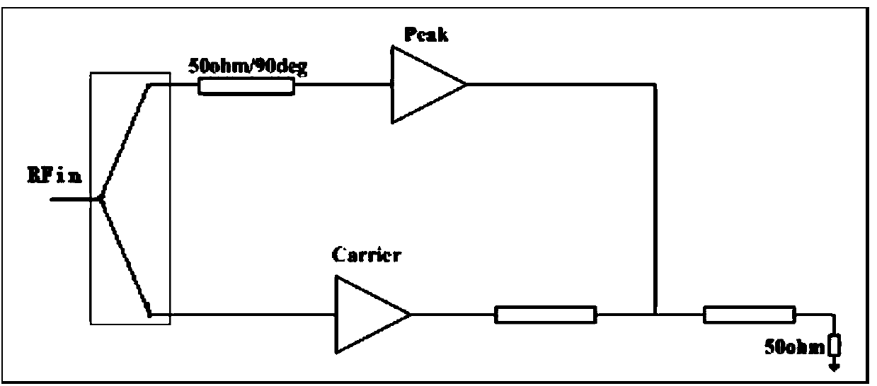
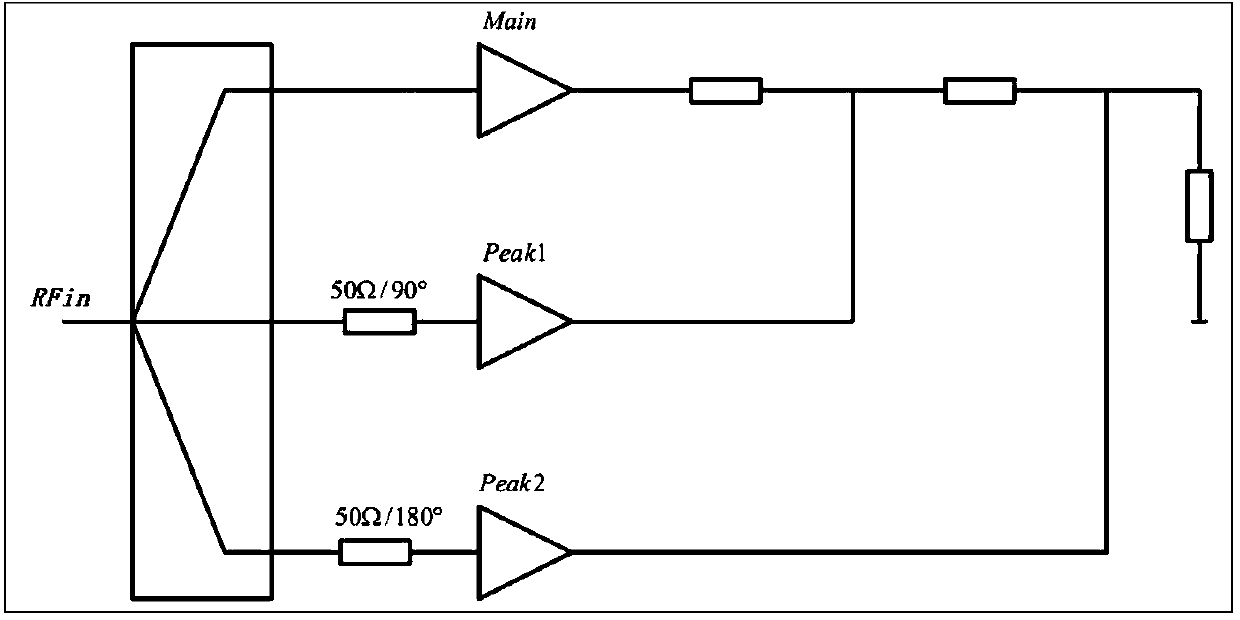
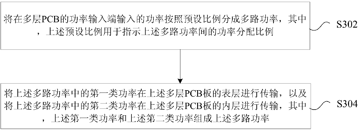
[0026] In this embodiment, a power distribution method in a multilayer PCB is provided, image 3 is a flowchart of a power distribution method in a multilayer PCB according to an embodiment of the present invention, such as image 3 As shown, the process includes the following steps:

[0027] Step S302, divide the power input at the power input terminal of the multilayer PCB into multiple power paths according to a preset ratio, wherein the preset ratio is used to indicate the power distribution ratio among the multiple power paths;

[0028] Step S304, transmitting the first type of power in the above multi-channel power on the surface layer of the above-mentioned multi-layer PCB board, and transmi...


PUM


Abstract

The invention provides a power distribution method of a multilayer printed circuit board PCB, an apparatus and a PCB thereof. The method comprises the following steps of dividing power input into a power input terminal of the multilayer PCB into multipath power according to a preset proportion, wherein the preset proportion is used for indicating a power distribution proportion among the multipath power; transmitting first class power in the multipath power on a surface layer of the multilayer PCB and transmitting second class power in the multipath power on an inner layer of the multilayer PCB, wherein the first class power and the second class power form the multipath power. By using the above technical scheme provided in the invention, problems that cost is high, a design is complex and a lot of PCB area is occupied during a power distribution process of the multilayer PCB in a correlation technology are solved; the power distribution can be designed to be performed among different layers of the PCB and the cost is saved; and simultaneously, an advantage of a multilayer board is fully used so that PCB layout is reasonable.

Description

technical field [0001] The present invention relates to the communication field, in particular, to a multilayer printed circuit board (Printed Circuit Board, PCB for short) power distribution method and device, and the PCB. Background technique [0002] In the face of increasingly fierce competition in the communication market, the efficiency of base station products has become the focus of competition in the industry. Power amplifier products are the main components of base stations. While their efficiency continues to improve, Doherty's architecture is becoming more and more complex. Moreover, as customers put forward more new requirements, such as: increasing the time slot shutdown function, increasing the receiving link, etc., the layout area of ​​the PCB is becoming more and more tight, and the conventional two-layer board can no longer meet the demand. More and more power amplifiers are designed with multi-layer boards. [0003] A traditional two-way Doherty power amp...

Claims


Application Information

Patent Timeline
Patent Type & Authority Applications(China)
IPC IPC(8): H05K1/02
CPCH05K1/02
Inventor 安晋元张璠王刚崔晓俊
Owner ZTE CORP
Why Eureka
Try Eureka