Optical image capturing system
An optical imaging system, image-side technology, applied in optics, optical components, instruments, etc., can solve problems such as manufacturing difficulties, increased distortion rate, and deterioration of peripheral imaging quality, achieve optimal optical path adjustment capabilities, improve imaging quality, and improve overall quality. Pixel vs. Quality Effects
- Summary
- Abstract
- Description
- Claims
- Application Information
AI Technical Summary
Problems solved by technology
Method used
Image

Examples
Embodiment approach
[0110] The sum of the focal lengths fp of each lens with positive refractive power in the optical imaging system is ΣPP, and the sum of the focal lengths of each lens with negative refractive power is ΣNP. An embodiment of the optical imaging system provided by the present invention satisfies the following Conditions: 0<ΣPP≦200; and f1 / ΣPP≦0.85. Preferably, the following conditions can be satisfied: 0<ΣPP≦150; and 0.01≦f1 / ΣPP≦0.6. Thereby, it is helpful to control the focusing ability of the optical imaging system, and properly distribute the positive refractive power of the system to suppress the premature occurrence of significant aberrations. The following conditions are simultaneously satisfied: ΣNP<-0.1; and f5 / ΣNP≦0.85. Preferably, the following conditions can be satisfied: ΣNP<0; and 0.01≦f5 / ΣNP≦0.5. Helps control the overall refractive power and overall length of the optical imaging system.
[0111] The first lens has positive refractive power, and its object side c...
no. 1 example
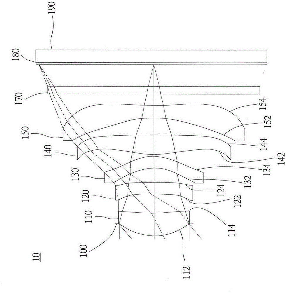
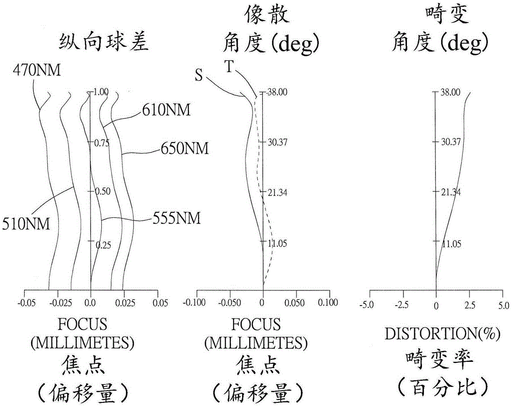
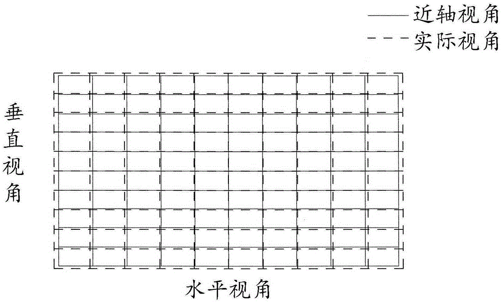
[0143] Such as Figure 1A and Figure 1B shown, where Figure 1A is a schematic diagram of an optical imaging system according to the first embodiment of the present invention, Figure 1B From left to right are the spherical aberration, astigmatism and optical distortion curves of the optical imaging system of the first embodiment. Figure 1C It is a TV distortion curve diagram of the optical imaging system of the first embodiment. Depend on Figure 1A It can be seen that the optical imaging system includes a first lens 110, an aperture 100, a second lens 120, a third lens 130, a fourth lens 140, a fifth lens 150, an infrared filter 170, and an imaging surface from the object side to the image side in sequence. 180 and an image sensing element 190 .
[0144] The first lens 110 has positive refractive power and is made of plastic material. The object side 112 is convex, and the image side 114 is concave, both of which are aspherical. The image side 114 has an inflection point...
no. 2 example
[0187] Such as Figure 2A and Figure 2B shown, where Figure 2A It is a schematic diagram of an optical imaging system according to the second embodiment of the present invention, Figure 2B From left to right are the spherical aberration, astigmatism and optical distortion curves of the optical imaging system of the second embodiment. Figure 2C It is a TV distortion curve diagram of the optical imaging system of the second embodiment. Depend on Figure 2A It can be seen that the optical imaging system includes a first lens 210, an aperture 200, a second lens 220, a third lens 230, a fourth lens 240, a fifth lens 250, an infrared filter 270, and an imaging surface from the object side to the image side in sequence. 280 and the image sensing element 290.
[0188] The first lens 210 has positive refractive power and is made of plastic material. The object side 212 is convex, and the image side 214 is concave, both of which are aspherical. Both the object side 212 and the ...
PUM
 Abstract
Description
Claims
Application Information
 - Generate Ideas
- Intellectual Property
- Life Sciences
- Materials
- Tech Scout
- Unparalleled Data Quality
- Higher Quality Content
- 60% Fewer Hallucinations
Browse by: Latest US Patents, China's latest patents, Technical Efficacy Thesaurus, Application Domain, Technology Topic, Popular Technical Reports.
© 2025 PatSnap. All rights reserved.Legal|Privacy policy|Modern Slavery Act Transparency Statement|Sitemap|About US| Contact US: help@patsnap.com