Method for scanning error bits

A technology for scanning errors and error bits, which is applied in the field of scanning error bits, can solve problems that affect the yield rate of memory chips, cannot set test conditions, and cannot match the read cycle of ECC error correction capability storage units, etc.

Active Publication Date: 2016-05-25
GIGADEVICE SEMICON (BEIJING) INC
View PDF5 Cites 2 Cited by
  • Summary
  • Abstract
  • Description
  • Claims
  • Application Information

AI Technical Summary

Problems solved by technology

However, when the actual controller uses ECC, it will arrange memory data and store ECC according to its own needs. During the test, it is impossible to set the corresponding test conditions according to the number of error bits in the storage

Method used


Image

  • Method for scanning error bits
  • Method for scanning error bits
  • Method for scanning error bits

Examples


Embodiment 1

[0026] Figure 5 It is a flow chart of a method for scanning error bits provided by Embodiment 1 of the present invention. This embodiment is applicable to the case of counting the number of error bits in data partitions of storage units. join Figure 5 The method for scanning error bits provided in this embodiment specifically includes the following steps:

[0027] S1. Divide the first data partition of the storage unit into N equal second data partitions on average, where N is a positive integer;

[0028] S2. Form a third data partition from the second data partition and scan the third data partition, and set the number of allowable error bits;

[0029] Preferably, forming the third data partition from the second data partition specifically includes forming a third data partition every four second data partitions, and of course, forming a third data partition every five second data partitions, It is not limited here.

[0030] Wherein, the number of allowable error bits i...

Embodiment 2

[0039] Image 6 The flow chart of a method for scanning error bits provided in Embodiment 2, on the basis of the above embodiments, step S2 is optimized in this embodiment. The advantage of such optimization is that the scanning of all second data partitions can be completed. see Image 6 The method for scanning error bits provided in this embodiment may specifically include the following:

[0040] S21. Divide the first data partition of the storage unit into N equal second data partitions on average, where N is a positive integer;

[0041] S221. First select all the second data partitions in the first data partition to form the third data partition, scan the third data partition, and set the number of allowable error bits, and continue to execute step S23;

[0042] S222. According to the arrangement order of the second data partitions, move the position of one second data partition backwards to form a third data partition, scan the third data partition, and set the number of...

Embodiment 3

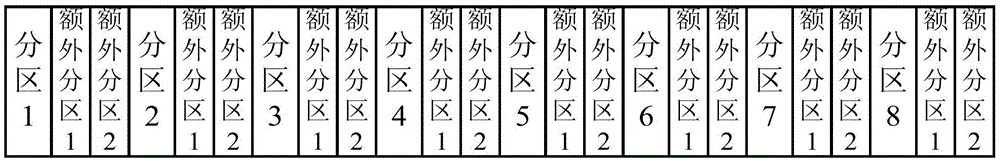
[0048] Figure 7 It is a schematic diagram of a scanning partition provided by Embodiment 3 of the present invention. On the basis of the above embodiments, this embodiment is as follows: figure 1 The page data partition of a storage unit in the prior art shown is scanned. see Figure 7 The method for scanning error bits provided in this embodiment may specifically include the following:

[0049] S31. Divide the first data partition of the storage unit into N equal second data partitions 2, wherein N is a positive integer;

[0050] The first data partition in this embodiment is specifically figure 1 Partition 1, Partition 2, Partition 3, Partition 4, Partition 5, Partition 6, Partition 7, Partition 8, Extra Partition 1, Extra Partition 2 are shown; N is 40.

[0051] S321. First select all the second data partitions in the first data partition to form the third data partition, scan the third data partition, and set the number of allowable error bits, and continue to execute...


PUM


Abstract

The invention discloses a method for scanning error bits. The method comprises the following steps: S1, averagely dividing a first data partition of a storage unit into N equal second data partitions; S2, forming a third data partition by using the second data partitions, scanning the third data partition and setting the permissible number of the error bits; S3, comparing the actual number of the error bits of the third data partition with the permissible number of the error bits, if the actual number of the error bits is greater than the permissible number of the error bits, executing step 4, if not, executing step 5; S4, carrying out one-time programming operation on the storage unit and returning to carry out the step S3; and S5, recording the current actual number of the error bits of the third data partition. According to the method, the qualification rate of storage chips can be adjusted through modifying the setting conditions; the corresponding data region and the error correcting capability of the own ECC (Error Correction Code) of a controller can be adjusted on the basis of final statistical results; and therefore, a better write performance is obtained.

Description

technical field [0001] The embodiment of the present invention relates to the field of storage technologies, and in particular to a method for scanning error bits. Background technique [0002] Non-volatile flash memory (norflash / nandflash) is a very common memory chip, which has the advantages of random access memory (RAM) and read-only memory (Read-Only Memory, ROM). Data will not be lost when power is off. A memory that can be electrically erased and written in the system, and its high integration and low cost make it the mainstream of the market. The Flash chip is composed of thousands of internal storage units, multiple storage units form a page, and multiple pages form a block. It is precisely because of this special physical structure that reading and writing are performed in units of pages in norflash / nandflash Data is erased in units of blocks. [0003] Due to the various crosstalk characteristics of the memory chip, error bits will appear during use. In order to ...

Claims


Application Information

Patent Timeline
IPC IPC(8): G06F11/10
CPCG06F11/1044G06F11/1072
Inventor 刘会娟苏志强
Owner GIGADEVICE SEMICON (BEIJING) INC
Why Eureka
Try Eureka