Method for forming semiconductor device and semiconductor device

A technology of semiconductors and devices, applied in the field of semiconductor manufacturing

Active Publication Date: 2016-05-25
INFINEON TECH AG
View PDF2 Cites 0 Cited by
  • Summary
  • Abstract
  • Description
  • Claims
  • Application Information

AI Technical Summary

Problems solved by technology

Realization of semiconductor substrates with diff

Method used


Image

  • Method for forming semiconductor device and semiconductor device
  • Method for forming semiconductor device and semiconductor device
  • Method for forming semiconductor device and semiconductor device

Examples


Embodiment Construction

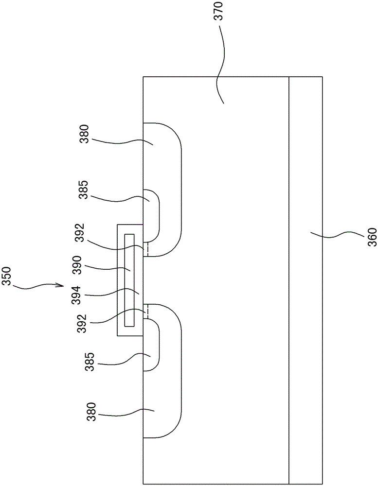
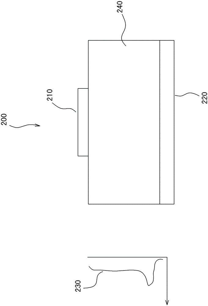
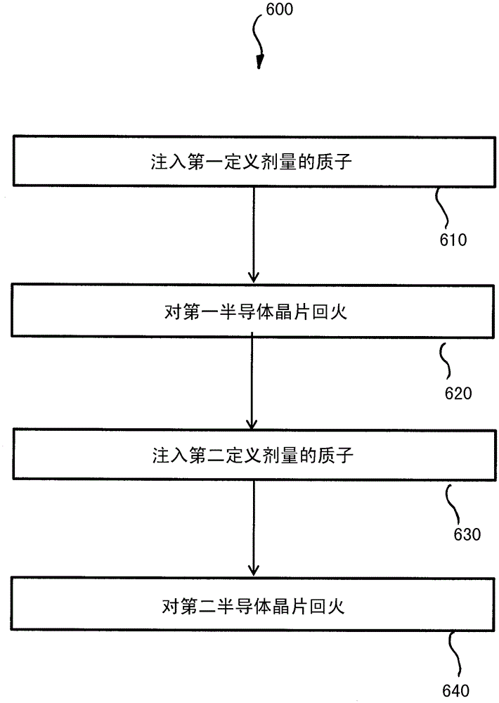
[0016] Various example embodiments will now be described more fully with reference to the accompanying drawings, in which some example embodiments are shown. In the drawings, the thickness of lines, layers and / or regions may be exaggerated for clarity.

[0017] Accordingly, while the example embodiments are capable of various modifications and alternative forms, embodiments thereof are shown as examples in the drawings and will be described in detail herein. It should be understood, however, that there is no intention to limit example embodiments to the particular forms disclosed, but on the contrary, example embodiments are to cover all modifications, equivalents, and alternatives falling within the scope of the disclosure. Throughout the description of the figures, like numerals refer to like or analogous elements.

[0018] It will be understood that when an element is referred to as being "connected" or "coupled" to another element, it can be directly connected or coupled ...


PUM

PropertyMeasurementUnit
Thicknessaaaaaaaaaa

Abstract

A method for forming a semiconductor device comprises implanting a defined dose of protons into a semiconductor substrate and tempering the semiconductor substrate according to a defined temperature profile. At least one of the defined dose of protons and the defined temperature profile is selected depending on a carbon-related parameter indicating information on a carbon concentration within at least a part of the semiconductor substrate.

Description

technical field [0001] Embodiments relate to semiconductor fabrication techniques, and in particular, to a method for forming a semiconductor device and a semiconductor device. Background technique [0002] Many semiconductor devices include a semiconductor substrate having regions of different conductivity types and different doping concentrations. Realization of semiconductor substrates with differently doped regions is often a challenging task. One way to generate donors in semiconductors is to implant protons to generate hydrogen-induced donors. It is desirable to increase the doping efficiency of donors by proton implantation. Contents of the invention [0003] Some embodiments relate to methods for forming semiconductor devices. The method includes implanting a defined dose of protons into the semiconductor substrate and tempering the semiconductor substrate according to a defined temperature profile. At least one of a defined dose of protons and a defined temper...

Claims


Application Information

Patent Timeline
IPC IPC(8): H01L21/265H01L21/331H01L29/739
CPCH01L21/265H01L29/66325H01L29/7393H01L21/263H01L22/12H01L22/14H01L22/20H01L29/66333H01L29/66348H01L29/7397H01L29/7395H01L29/36H01L21/324H01L29/1095
Inventor M.耶利内克J.G.拉文H.厄夫纳H-J.舒尔策W.舒斯特雷德
Owner INFINEON TECH AG
Why Eureka
Try Eureka