
An embedded memory emb configuration chain structure and configuration method

An embedded memory, configuration chain technology, applied in static memory, digital memory information, information storage and other directions, can solve problems such as unfavorable FPGA chip integration, and achieve the effect of reducing the number of interface lines, reducing complexity, and reducing wiring.

Active Publication Date: 2019-03-15
CAPITAL MICROELECTRONICS
View PDF4 Cites 0 Cited by
  • Summary
  • Abstract
  • Description
  • Claims
  • Application Information

AI Technical Summary

Problems solved by technology

[0005] However, with the continuous expansion of the FPGA chip scale, the number of EMB modules is also increasing. If the configuration port of each EMB is connected to the configuration control module for control, the number of these connections will be very large, which is very unfavorable. Integration of the top layer of the FPGA chip

Method used


Image

  • An embedded memory emb configuration chain structure and configuration method
  • An embedded memory emb configuration chain structure and configuration method
  • An embedded memory emb configuration chain structure and configuration method

Examples


Embodiment Construction

[0031] The technical solutions of the present invention will be described in further detail below with reference to the accompanying drawings and embodiments.

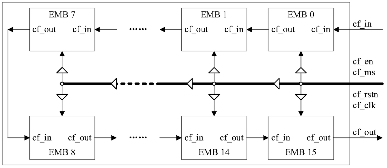
[0032] The EMB configuration chain provided by the embodiment of the present invention is composed of at least two EMBs that are cascaded. figure 1 It is a schematic diagram of an EMB configuration chain structure in an FPGA chip provided by an embodiment of the present invention. in such as figure 1 In the example shown, the EMB configuration chain includes 16 sequentially cascaded EMBs.

[0033] In the EMB configuration chain, the clock signal cf_clk, the configuration mode selection enable signal cf_ms, the enable signal cf-en, and the reset signal cf_rstn are transmitted from right to left through the buffer level by level as shown in the figure, and the configuration data input port Under the sampling of the clock signal cf_clk, the input data cf_in selects the setting of the enable signal cf_ms and the enable s...


PUM


Abstract

The present invention relates to an EMB configuration chain structure and a configuration method of a configuration chain. The configuration chain includes at least two EMBs that are cascaded. Each EMB includes a configuration controller and a static random access memory (SRAM). Input data of a configuration data input port of the EMB configuration chain is written in a corresponding SRAM according to control of the configuration controller of each EMB; and data stored in the SRAM of the current EMB is output to next cascaded EMB according to control of the configuration controller of the current EMB, or is output through the configuration data output port of the EMB configuration chain.

Description

technical field [0001] The invention relates to the technical field of integrated circuit design, in particular to an embedded memory EMB configuration chain structure and configuration method. Background technique [0002] For a field programmable gate array (Field Programmable Gate Array, FPGA) chip, an embedded memory (EMB) in the FPGA chip is a very important module. Generally speaking, the core of EMB is a dual-port static random access memory (SRAM). There will be many selectors (MUX) outside the SRAM to configure the working mode of the SRAM, including bit width, bit depth, clock (clock) selection, output Storage selection and other functions. [0003] After the FPGA chip is powered on, there are two modes: configuration mode and user mode. Usually, in the configuration mode, each configurable module inside the FPGA chip needs to be configured to a desired state, which also includes the configuration of the EMB. A common practice is to connect the configuration por...

Claims


Application Information

Patent Timeline
Patent Type & Authority Patents(China)
IPC IPC(8): G11C11/413
Inventor 李大伟刘明
Owner CAPITAL MICROELECTRONICS
Learn More