Bipolar junction transistor and related manufacturing method thereof

A bipolar junction, transistor unit technology, applied in transistors, semiconductor/solid-state device manufacturing, electric solid-state devices, etc., can solve the problems of increasing the mask layer manufacturing process, difficulty in implementation, and high manufacturing costs, and achieve simplified design and complexity. degree and cost, large magnification factor and magnification factor drop characteristics, the effect of small edge effect

Active Publication Date: 2016-06-01
CHENGDU MONOLITHIC POWER SYST
View PDF6 Cites 3 Cited by
  • Summary
  • Abstract
  • Description
  • Claims
  • Application Information

AI Technical Summary

Problems solved by technology

[0002] Existing vertical bipolar junction transistors (BJT) usually have poor isolation performance from the substrate or well region, which will cause unwanted carrier injection into the substrate and the formation of parasitic BJTs
In order to improve the isolation performance, it is usually necessary to make a deep buried layer to completely surround the vertical BJT, but this requires an additional mask layer and a more complicated manufacturing process to make the deep buried layer
Relatively difficult to implement and expensive to produce

Method used


Image

  • Bipolar junction transistor and related manufacturing method thereof
  • Bipolar junction transistor and related manufacturing method thereof
  • Bipolar junction transistor and related manufacturing method thereof

Examples


Embodiment Construction

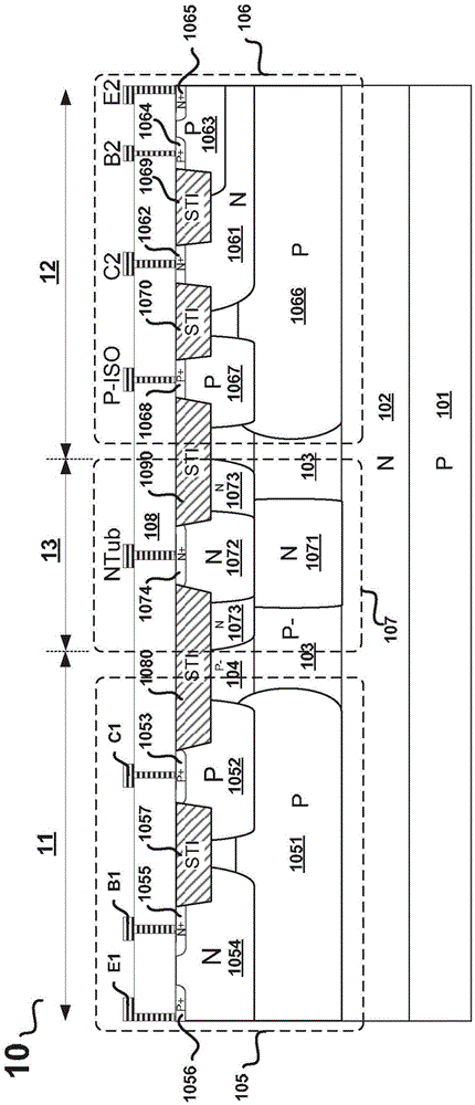
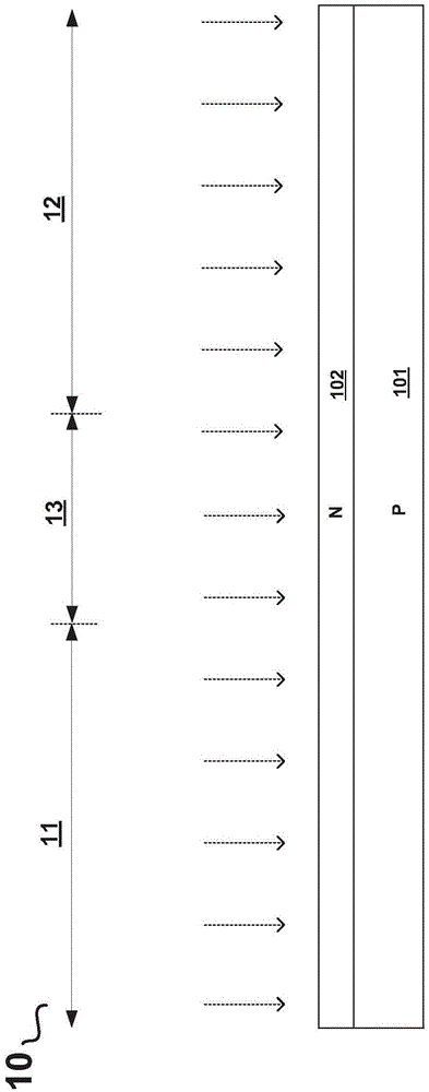
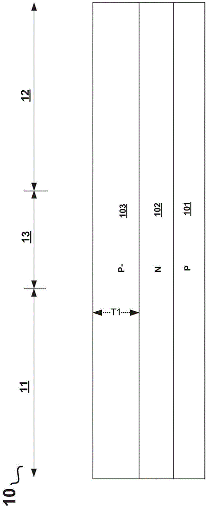
[0010] Some embodiments of the present disclosure will be described in detail below with reference to the accompanying drawings. It should be understood, however, that these descriptions are exemplary only, and are not intended to limit the scope of the present disclosure. Also, descriptions of well-known structures and techniques are omitted in the following description to avoid unnecessarily obscuring the concepts of the present disclosure.

[0011] In the following description, some specific details, such as the specific circuit structure, device structure, process steps and specific parameters of these circuits, devices and processes in the embodiments, are used to provide a better understanding of the embodiments of the present disclosure . It will be understood by those skilled in the art that the embodiments of the present disclosure may be practiced even without some details or in combination with other methods, elements, materials, and the like.

[0012] In the desc...


PUM


Abstract

The invention provides a bipolar junction transistor and a related manufacturing method thereof. According to the embodiment provided by the invention, the bipolar junction transistor comprises a first buried layer, a first epitaxial layer, a second epitaxial layer, a PNP bipolar junction transistor unit, an NPN bipolar junction transistor unit and a first isolating structure, wherein the first buried layer is formed in a semiconductor substrate; the first epitaxial layer and the second epitaxial layer are formed on the first buried layer; the PNP bipolar junction transistor unit, the NPN bipolar junction transistor unit and the first isolating structure are fabricated in the first epitaxial layer and the second epitaxial layer; the first isolating structure is located between the PNP bipolar junction transistor unit and the the NPN bipolar junction transistor unit and are connected with the first buried layer to form an isolating barrier. The isolating barrier not only can effectively isolate the PNP bipolar junction transistor unit from the NPN bipolar junction transistor unit, but also can effectively isolate the PNP bipolar junction transistor unit and the NPN bipolar junction transistor unit from the semiconductor substrate, and prevents a charge carrier from being injected into the substrate and a parasitic BJT from being formed.

Description

technical field [0001] Embodiments of the present disclosure relate to semiconductor devices, particularly but not limited to bipolar junction transistors and methods of manufacturing the same. Background technique [0002] Existing vertical bipolar junction transistors (BJTs) usually have poor isolation performance from the substrate or well region, which will cause unwanted carrier injection into the substrate and formation of parasitic BJTs. In order to improve the isolation performance, it is usually necessary to make a deep buried layer to completely surround the vertical BJT, but this requires an additional mask layer and a more complicated manufacturing process to make the deep buried layer. It is relatively difficult to realize and the production cost is high. In addition to the isolation performance and production cost, it is also hoped that the amplification factor (usually expressed by β) of the BJT is relatively high. Contents of the invention [0003] To sol...

Claims


Application Information

Patent Timeline
Patent Type & Authority Applications(China)
IPC IPC(8): H01L27/082H01L21/8228
CPCH01L21/82285H01L21/761H01L27/0826H01L29/0653H01L29/0821H01L29/107H01L29/732
Inventor 连延杰傅达平吉杨永
Owner CHENGDU MONOLITHIC POWER SYST
Why Eureka
Try Eureka