Offset Voltage Elimination Circuit Structure for Dimming Device Protection Mechanism

A protection mechanism, offset voltage technology, applied in the direction of lamp circuit layout, lighting device, light source, etc., can solve the problems affecting GD pulse output, voltage offset, etc.

Active Publication Date: 2019-06-21
昱京能源科技股份有限公司
View PDF6 Cites 0 Cited by
  • Summary
  • Abstract
  • Description
  • Claims
  • Application Information

AI Technical Summary

Problems solved by technology

[0011] However, in practical applications, a current-limiting resistor is usually set at the above-mentioned dimming signal input terminal Adj_in to protect the constant current source A and related circuits from damage caused by excessive voltage or reverse voltage polarity; therefore, in Under normal use conditions (especially for resistive dimmers, the dimming signal voltage input from the dimming signal input terminal Adj_in is formed by a constant current source A outputting a current on a variable resistor RT), any current Flowing through the current-limiting resistor will inevitably produce a voltage drop of the current-limiting resistor. The voltage drop of the current-limiting resistor is added to the voltage introduced or generated by the dimming signal input terminal Adj_in, and a voltage offset (offset) will be generated. This voltage The offset will affect the GD pulse output (dimming control voltage) output by the subsequent hysteresis comparator CMP1, so it must be eliminated in order to obtain the real required dimming signal voltage input

Method used


Image

  • Offset Voltage Elimination Circuit Structure for Dimming Device Protection Mechanism
  • Offset Voltage Elimination Circuit Structure for Dimming Device Protection Mechanism
  • Offset Voltage Elimination Circuit Structure for Dimming Device Protection Mechanism

Examples


Embodiment Construction

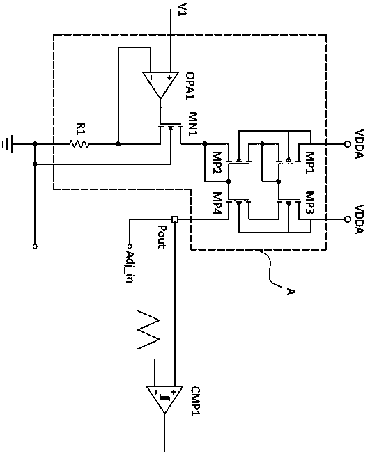
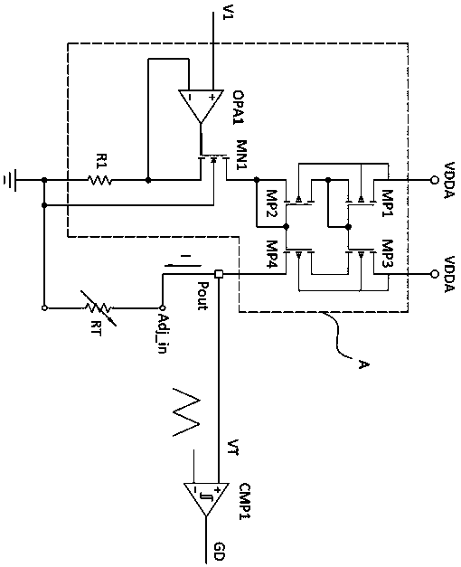
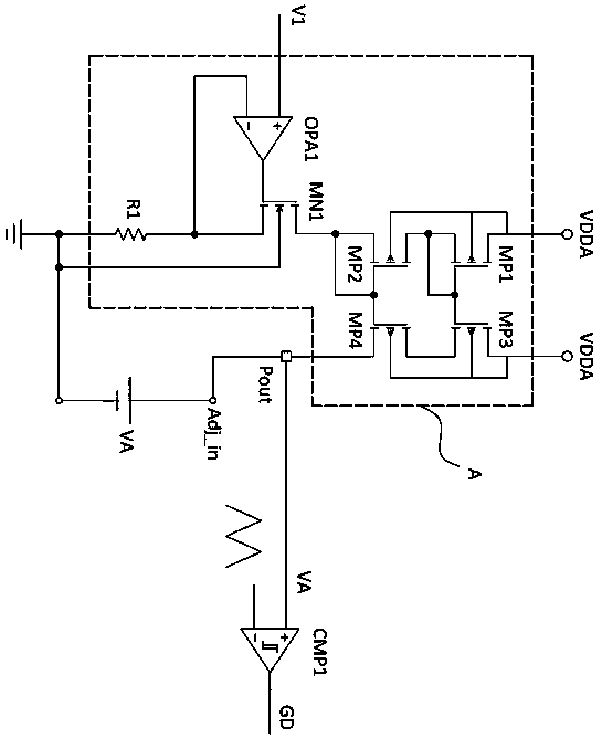
[0031] Please refer to Figure 5 As shown, it can be seen that the circuit structure of the present invention mainly includes parts such as a constant current source A, a subtractor B and a hysteresis comparator CMP1, wherein the constant current source A is composed of mutually symmetrical P-type crystals MP1, MP2, and MP3 , MP4 and an N-type crystal MN1 composed of a cascaded current mirror circuit, in addition to a first operational amplifier OPA1, a first resistor R1, the non-inverting input of the first operational amplifier OPA1 can be input A voltage V1, the inverting input terminal of the first operational amplifier OPA1 can be connected to the G pole of the N-type crystal MN1, and grounded through the first resistor R1, and the S pole of the P-type crystal MP4 is connected to an output terminal Pout, and the output terminal Pout In addition, a dimming signal input terminal Adj_in is connected via a current limiting resistor RL.

[0032] The subtractor B is made up of...


PUM


Abstract

An offset voltage cancellation circuit structure of a dimming apparatus protection mechanism is disclosed. The offset voltage cancellation circuit mainly comprises a constant current source capable of outputting constant current; the output end of the constant current source is connected with a dimming signal input end through a current-limiting resistor; the dimming signal input end is connected with an external conventional dimmer output end; when current passes through the current-limiting resistor, a current-limiting resistance voltage that causes voltage offset is generated; an input end of a subtracter is communicated with the constant current source; an offset reference voltage can be imported into another input end of the subtracter; a non-inverted input end of a hysteresis comparator is connected to the output end of the subtracter; and a sawtooth wave can be input to the inverted input end of the hysteresis comparator. Therefore, the offset reference voltage is set to be equal to the current-limiting resistance voltage; the current-limiting resistance voltage can be cancelled by the subtracter, so that the hysteresis comparator can obtain a correct dimming signal voltage, and a GD pulse signal capable of adjusting the luminance of light rays is output.

Description

[0001] Technical field: [0002] The present invention relates to an offset voltage elimination circuit structure for the protection mechanism of a dimming device, in particular to a structure that can provide current output when connecting an external resistor type dimmer, and effectively eliminate the external current limiting resistor used for the protection circuit. Circuit configuration for voltage difference (offset). [0003] Background technique: [0004] Light-emitting diodes (LEDs) have the characteristics of low energy consumption and long service life, so they have gradually been matured and widely used in various lighting requirements; however, due to the great differences between LED light source components and traditional light source Physical characteristics are different, and the dimming circuit suitable for traditional light source components cannot directly control the brightness change of LED light source components, so a conversion circuit is used to connec...

Claims


Application Information

Patent Timeline
IPC IPC(8): H05B37/02
Inventor 杨森泰
Owner 昱京能源科技股份有限公司
Why Eureka
Try Eureka