Wafer Grinding Method

A grinding method and wafer technology, applied in the direction of grinding machine tools, grinding devices, manufacturing tools, etc., can solve problems affecting chip quality, damage, etc., and achieve the effect of reducing structural damage

Active Publication Date: 2020-06-09
SEMICON MFG INT (SHANGHAI) CORP
View PDF6 Cites 0 Cited by
  • Summary
  • Abstract
  • Description
  • Claims
  • Application Information

AI Technical Summary

Problems solved by technology

[0005] However, even so, after the wafer BG process, after removing the protective tape on the functional surface of the wafer, it was found that the functional surface of the wafer was still damaged (Peeling), which affected the chip quality

Method used


Image

  • Wafer Grinding Method
  • Wafer Grinding Method
  • Wafer Grinding Method

Examples


Embodiment Construction

[0028] As mentioned in the background art, in the back grinding process of existing wafers, even if the functional surface of the wafer is covered with a protective tape (BG tape), after the protective tape is removed, it is found that the functional surface of the wafer is still damaged. Analyze its reasons:

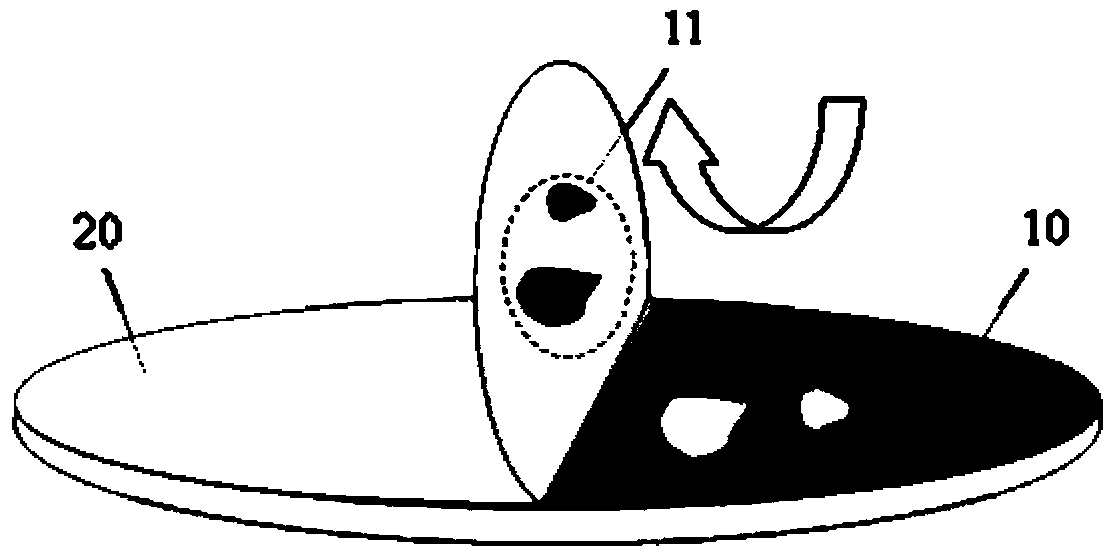
[0029] The existing protective tape is adhered to the functional surface of the wafer, and the protective tape and the wafer have strong adhesion to prevent the protective tape from falling off during the grinding process, thereby better protecting the functional surface of the wafer from contamination. And damage caused by direct contact with grinding equipment. But after the grinding process, refer to figure 1 , due to the strong adhesion between the protective tape 20 and the wafer 10, during the process of tearing off the protective tape 20 from the functional surface of the wafer 10, the protective tape 20 will damage parts 11 on the surface of the functional surf...


PUM


Abstract

The invention provides a wafer grinding method. The wafer grinding method includes the steps that a wafer is provided and comprises a functional face and a back face opposite to the functional face; after a protective layer is formed on the functional face of the wafer, the protective layer is covered with a layer of protective adhesive tape; then, the wafer is placed on a grinding device, the back face of the wafer is ground so that the portion, with the partial thickness, of the wafer can be removed; and the protective adhesive tape is removed, and then the protective layer is removed. Before grinding, the protective layer is formed on the functional face of the wafer, and then the protective layer is covered with one layer of protective adhesive tape. In the grinding process of the protective adhesive tape, the structure on the functional face of the wafer can be effectively protected against damage in the grinding process, the protective adhesive tape is pasted on the protective layer, the situation that the protective adhesive tape makes contact with the functional face of the wafer can be effectively avoided, and therefore in the process of tearing off the adhesive tape after the grinding technology, the protective adhesive tape can remove defects of parts on the surface of the functional face of the part of the wafer, and structural damage on the functional face of the wafer is reduced.

Description

technical field [0001] The invention relates to the field of semiconductors, in particular to a wafer grinding method. Background technique [0002] With the development of science and technology, the functions of electronic products continue to increase, while the size continues to decrease. In the field of semiconductor device manufacturing, the size of semiconductor devices is continuously reduced, and the size of electronic chips is continuously reduced. [0003] For this reason, in the semiconductor device manufacturing process, after many semiconductor devices are formed on the functional surface of the wafer, the wafer back grinding process (Back Grinding, referred to as BG) is performed, and the wafer corresponding to the functional surface is ground by a planarization process. Part of the thickness of the wafer is removed on the back side to reduce the thickness of the subsequently formed chip. [0004] In the process of grinding the back of the wafer, a layer of ...

Claims


Application Information

Patent Timeline
Patent Type & Authority Patents(China)
IPC IPC(8): B24B37/04B24B1/00H01L21/02H01L21/683
Inventor 陈彧
Owner SEMICON MFG INT (SHANGHAI) CORP
Why Eureka
Try Eureka