CMOS power amplifier matching circuit

A power amplifier and matching circuit technology, which is applied in the direction of amplifiers, amplifier input/output impedance improvement, amplifier parts, etc., can solve the problems of increasing the difficulty of PCB design, and the internal matching network is not suitable for low frequency bands, etc.

Active Publication Date: 2016-06-08
WUHAN SYNTEK CO LTD
View PDF4 Cites 5 Cited by
  • Summary
  • Abstract
  • Description
  • Claims
  • Application Information

AI Technical Summary

Problems solved by technology

[0003] At present, the output matching network of CMOS power amplifiers basically adopts two types of on-chip and off-chip. The internal matching network is not suitable for low frequency bands, and the off-chip matching network increases the difficulty of PCB design.

Method used


Image

  • CMOS power amplifier matching circuit

Examples


Embodiment Construction

[0019] The following will clearly and completely describe the technical solutions in the embodiments of the present invention in conjunction with the accompanying drawings in the operating principle of the present invention. Obviously, the described embodiments are only some, not all, embodiments of the present invention. Based on the embodiments of the present invention, all other embodiments obtained by persons of ordinary skill in the art without creative efforts fall within the protection scope of the present invention.

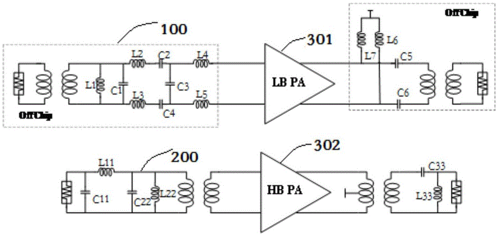
[0020] Please refer to figure 1 , a CMOS power amplifier matching circuit, the CMOS power amplifier matching circuit includes a circuit board, an off-chip matching network 100 arranged on the circuit board, and a power amplifier integrated chip arranged on the circuit board; the power amplifier integrated chip includes a high-frequency power amplifier 302. The low-frequency power amplifier 301 and the on-chip matching network 200, the high-frequency power...


PUM


Abstract

The invention discloses a CMOS power amplifier matching circuit. The CMOS power amplifier matching circuit comprises a circuit board and an extra-chip matching network and a power amplification integrated chip which are arranged on the circuit board; the power amplification integrated chip comprises a high frequency power amplifier, a low frequency power amplifier and an intra-chip matching network, the high frequency power amplifier is connected with the intra-chip matching network, and the low frequency power amplifier is connected with the extra-chip matching network. The CMOS power amplifier matching circuit can integrate the advantages of the intra-chip matching network and the extra-chip matching network, and a PA is divided into a high frequency part and a low frequency part, wherein the high frequency part is achieved through the intra-chip matching network, and design difficulty of the PCB is decreased; the low frequency part is achieved through the extra-chip matching network, and good performance is achieved.

Description

technical field [0001] The invention relates to the field of power amplification, in particular to a CMOS power amplifier matching circuit. Background technique [0002] After entering the 21st century, the contradiction between energy demand and supply has become more and more prominent. All walks of life around the world are striving to achieve high-efficiency energy utilization. This puts forward high requirements for wireless communication integrated circuit systems, covering low-voltage, A series of relatively demanding indicators such as low power consumption, high performance, light weight, and small size. At present, mobile communication devices are all designed with digital-analog hybrid integrated circuits, that is, the front-end RF receiving circuit part is an analog system, and the part after the back-end A / D converter is a digital system. Due to the requirements of low voltage, low power consumption and small size, the single-chip integration of the front-end a...

Claims


Application Information

Patent Timeline
Patent Type & Authority Applications(China)
IPC IPC(8): H03F1/56
CPCH03F1/565
Inventor 张科峰任达明
Owner WUHAN SYNTEK CO LTD
Why Eureka
Try Eureka