Pixel circuit and driving method thereof, array substrate, display panel and display device

A technology of a pixel circuit and a driving method, applied in the display field, can solve the problems of inability to compensate the threshold voltage of the driving transistor, poor brightness uniformity of the display panel, etc.

Active Publication Date: 2016-06-15
BOE TECH GRP CO LTD +1
View PDF5 Cites 78 Cited by
  • Summary
  • Abstract
  • Description
  • Claims
  • Application Information

AI Technical Summary

Problems solved by technology

[0004] The main purpose of the present invention is to provide a pixel circuit and its driving method, an array substrate and a display device, which solves the problem that in the prior art, only the gate of the driving tra...

Method used


Image

  • Pixel circuit and driving method thereof, array substrate, display panel and display device
  • Pixel circuit and driving method thereof, array substrate, display panel and display device
  • Pixel circuit and driving method thereof, array substrate, display panel and display device

Examples


Embodiment Construction

[0075] The following will clearly and completely describe the technical solutions in the embodiments of the present invention with reference to the accompanying drawings in the embodiments of the present invention. Obviously, the described embodiments are only some, not all, embodiments of the present invention. Based on the embodiments of the present invention, all other embodiments obtained by persons of ordinary skill in the art without making creative efforts belong to the protection scope of the present invention.

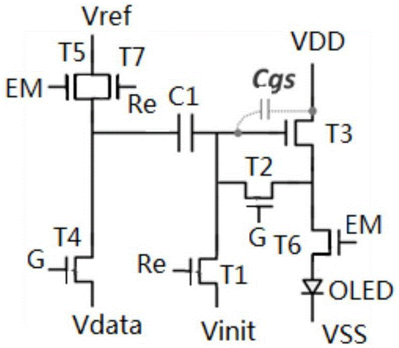
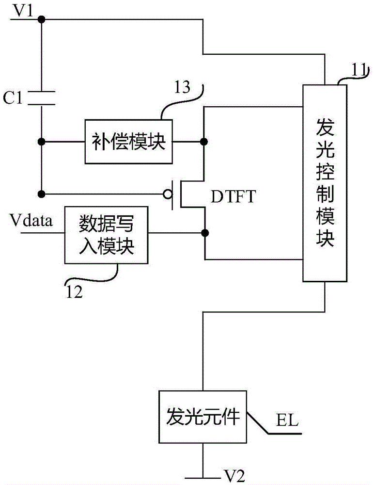
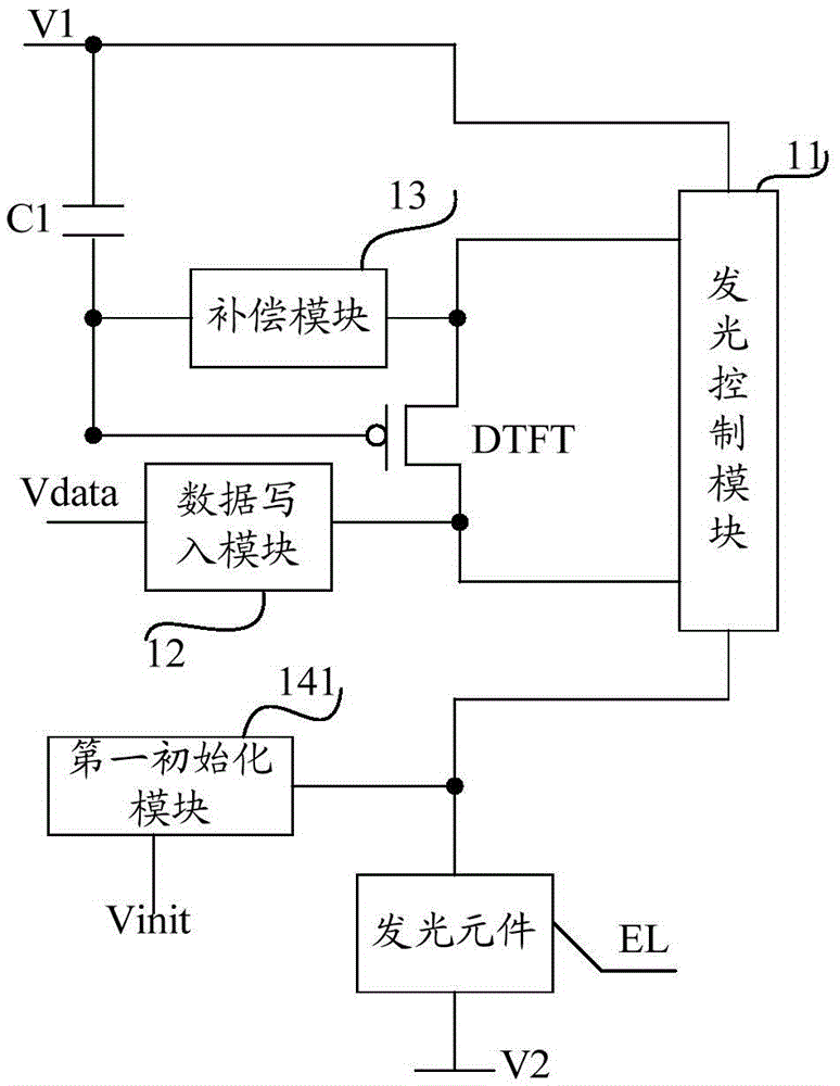
[0076] Such as figure 2 As shown, the pixel circuit described in the embodiment of the present invention includes a light emitting element EL, a driving transistor DTFT, a first storage capacitor C1, a light emitting control module 11, a data writing module 12 and a compensation module 13, wherein,

[0077] The first terminal of the first storage capacitor C1 is connected to the gate of the driving transistor DTFT, and the second terminal of the first storage...


PUM


Abstract

The invention provides a pixel circuit and a driving method thereof, an array substrate, a display panel and a display device. The pixel circuit comprises a light-emitting component, a driving transistor, a first storage capacitor, a light-emitting control module, a data write-in module and a compensation module. The data write-in module controls data voltage Vdata to be written into a second pole of the driving transistor in the compensation stage; and the compensation module controls a first pole of the driving transistor to be connected with the grid electrode of the driving transistor in the compensation stage to control the driving transistor to be conducted and control the conduction current of the driving transistor to flow from the second pole of the driving transistor to the first pole of the driving transistor until the electric potential of the grid electrode of the driving transistor is Vdata+Vth, wherein the Vth is a threshold voltage of the driving transistor. The problem that the threshold voltage of the driving transistor cannot be compensated in the light-emitting stage, and thus uniformity of brightness of the display panel is poor in the prior art is solved.

Description

technical field [0001] The present invention relates to the field of display technology, in particular to a pixel circuit and a driving method thereof, an array substrate, a display panel and a display device. Background technique [0002] AMOLED (ActiveMatrixOrganicLightEmittingDiode, Active Matrix Organic Light Emitting Diode) can be driven by the current generated by the driving transistor in the saturated state, because when the same gray scale voltage is input, different threshold voltages of the driving transistor will lead to different Drive current, causing current inconsistency. However, the uniformity of the threshold voltage Vth on the LTPS (low temperature polysilicon technology) process is very poor, and Vth also drifts, so the brightness uniformity of the existing pixel driving circuit has always been poor. [0003] Such as figure 1 As shown, the existing pixel circuit includes a first transistor T1, a second transistor T2, a third transistor T3, a fourth tra...

Claims


Application Information

Patent Timeline
IPC IPC(8): G09G3/3208
CPCG09G3/3258G09G3/3233G09G2310/0251G09G2310/0262G09G2300/0861G09G2320/045G09G2300/0819G09G3/325G09G2300/0876G09G2320/0233
Inventor 高永益王博陈义鹏张毅
Owner BOE TECH GRP CO LTD
Why Eureka
Try Eureka