Reverse conducting MOS gate-controlled thyristor and fabrication method thereof

A reverse-conducting, thyristor technology, applied in the field of power semiconductor devices, can solve problems such as adverse effects of forward conduction, voltage stagnation, and device damage, and achieve the effects of suppressing the snapback effect, large current conduction capability, and reducing the effective area.

Active Publication Date: 2016-06-15
UNIV OF ELECTRONICS SCI & TECH OF CHINA
View PDF4 Cites 18 Cited by
  • Summary
  • Abstract
  • Description
  • Claims
  • Application Information

AI Technical Summary

Problems solved by technology

Taking the pulse discharge circuit as an example, if there is no reverse conduction capability, the continuous pulse process cannot be realized, and the reverse will cause voltage stagnation, and the energy is difficult to be released smoothly, and device damage is prone to occur
[0004] In order to solve this problem, a reverse conducting MGT (Reverse Conducting MGT), referred to as RC-MGT, was proposed, such as figure 1 It shows that by introducing a short-circuit area at the anode and cathode at the same time, a current channel is designed for its reverse conduction. The characteristics are similar to a diode, but the structure will cause the MGT to have two snapback phenomena when it works in the forward direction. The first is the anode short circuit. The switch from unipolar operation to bipolar operation is caused by the switch, and the second time is the switch from triode operation to thyristor operation due to the cathode short circuit structure.
These two snapbacks adversely affected its forward conduction

Method used


Image

  • Reverse conducting MOS gate-controlled thyristor and fabrication method thereof
  • Reverse conducting MOS gate-controlled thyristor and fabrication method thereof
  • Reverse conducting MOS gate-controlled thyristor and fabrication method thereof

Examples


Embodiment Construction

[0033] Below in conjunction with accompanying drawing, describe technical scheme of the present invention in detail:

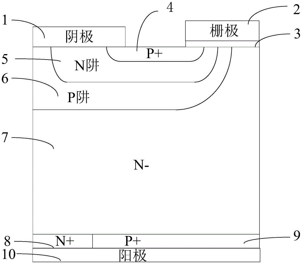
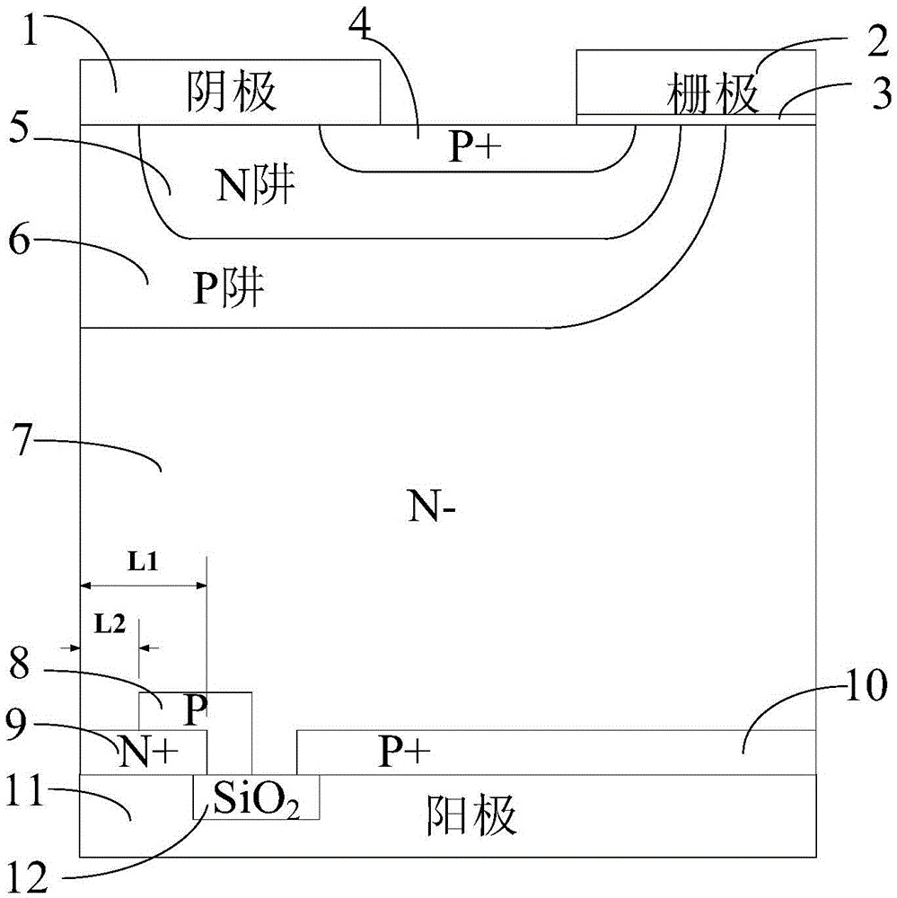
[0034] figure 2 It is a structural schematic diagram of a reverse conduction type MOS gate-controlled thyristor of the present invention. As shown in the figure, it includes metallized cathode 1, gate electrode 2, gate oxide layer 3, P well 4, N well 5, P well 6, N drift region 7, P floating layer 8, N anode region 9, and P anode Region 10, metallized anode 11 and anode isolation oxide layer 12; P well 6 is located on top of N drift region 7, N well 5 is located in P well 6, P well 4 is located in N well 5, gate oxide layer 3 is located in N well 5 , the surfaces of the P well 6 and the N drift region 7, the gate electrode 2 is located on the surface of the gate oxide layer 3, and the metallized cathode 1 covers the N well 5, the P well 6 and a part of the P well 4. The lower surface of the N drift region 7 has a P floating region 8, between the P floating ...


PUM


Abstract

The invention belongs to the field of power semiconductor devices, and particularly relates to a reverse conducting MOS gate-controlled thyristor and a fabrication method thereof. The novel reverse conducting MOS gate-controlled thyristor provided by the invention can play a role of an electronic potential barrier when the current density is relatively low, so that the cell length of an N anode region is reduced; the effective area is reduced; the snapback effect is inhibited by greatly improving an anode short-circuit resistance; a P floating region also carries out hole emission towards an N drift region along with a voltage increase, so that conductivity modulation is carried out and the snapback effect is inhibited. Meanwhile, due to additionally introduced P floating region in reverse conduction, a parasitic PNPN structure is passed in conduction; the thyristor is conducted when a current reaches a certain magnitude; and the novel reverse conducting MOS gate-controlled thyristor also has high current conduction capability in the reverse direction.

Description

technical field [0001] The invention belongs to the field of power semiconductor devices, and in particular relates to a reverse conduction type MOS gate-controlled thyristor and a manufacturing method thereof. Background technique [0002] With the continuous development of human society, energy consumption is also increasing. While increasing output, there are higher and higher requirements for the utilization rate of electric energy. The realization of these requirements depends on the development of power electronic devices. As a new type of power device, MOS gate-controlled thyristor has also attracted everyone's attention. [0003] MOS Gated Thyristor (MOSGated Thyristor), referred to as MGT, is a composite device that combines the characteristics of MOSFET and thyristor. At the same time, it has the advantages of high input impedance of MOSFET, convenient gate-level control, high blocking voltage and low conduction voltage drop of thyristor, and is widely used in th...

Claims


Application Information

Patent Timeline
Patent Type & Authority Applications(China)
IPC IPC(8): H01L29/745H01L21/332H01L29/06H01L29/417
CPCH01L29/0684H01L29/41716H01L29/66363H01L29/7455
Inventor 陈万军李震洋蒋华平刘超古云飞程武张波
Owner UNIV OF ELECTRONICS SCI & TECH OF CHINA
Why Eureka
Try Eureka