
System and method for implementing frequency band compatibility

A technology to realize the system and frequency band, applied in the field of compatibility, can solve the problems of radio frequency line interference, limited number of receiving ports at the transceiver end, and difficulty in frequency band compatibility, etc., to achieve the effect of ensuring radio frequency performance

Active Publication Date: 2018-08-24
NINGBO SAGEREAL COMM
View PDF7 Cites 0 Cited by
  • Summary
  • Abstract
  • Description
  • Claims
  • Application Information

AI Technical Summary

Problems solved by technology

Therefore, in order to meet the needs of different customers, frequency band compatibility becomes very necessary. However, the number of receiving ports at the transceiver end is limited, the PCB layout area is particularly tight, and the RF wiring is particularly prone to interference due to compatibility, making current frequency band compatibility difficult.

Method used


Image

  • System and method for implementing frequency band compatibility
  • System and method for implementing frequency band compatibility
  • System and method for implementing frequency band compatibility

Examples


Embodiment 1

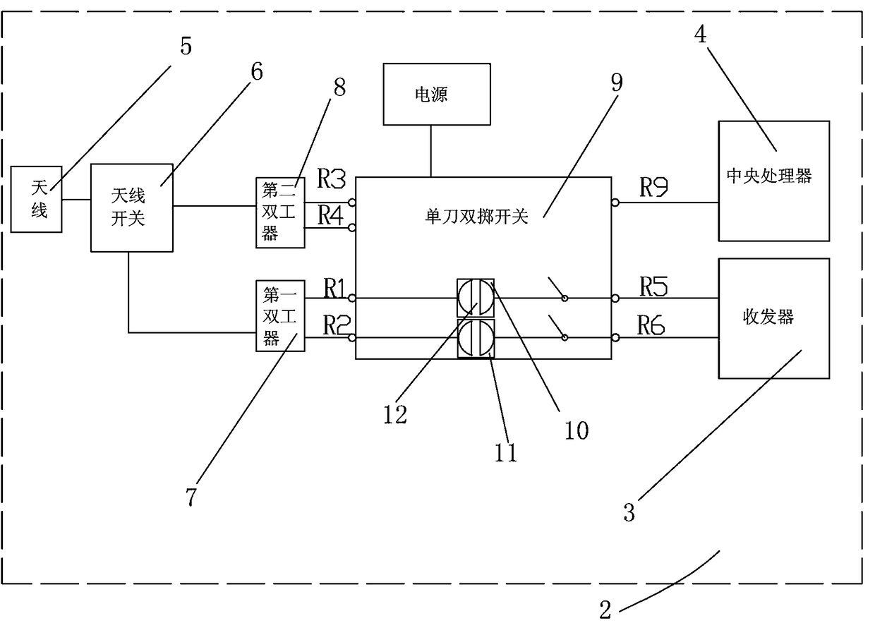
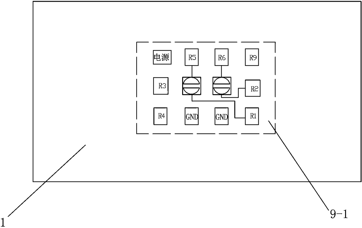
[0024] like figure 1 , figure 2 As shown, a frequency band compatible implementation system provided in this embodiment includes a PCB board 1 and a frequency band compatible circuit 2, and a wiring structure of the frequency band compatible circuit 2 is provided on the PCB board 1, and is characterized in that: The frequency band compatible circuit 2 includes a transceiver 3, a central processing unit 4, an antenna 5, an antenna switch 6, a first duplexer 7, a second duplexer 8, a single-pole double-throw switch 9, a first short-circuit pad 10 and a second Two short-circuit pads 11, the two input and output ports of the transceiver 3 are respectively connected to the sixth input and output port R6 pin and the fifth input and output port R5 pin of the single-pole double-throw switch 9, and the single-pole double-throw switch 9 The pin of the first input and output port R1 of the single pole double throw switch 9 is connected with the pin of the fifth input and output port R5...

Embodiment 2

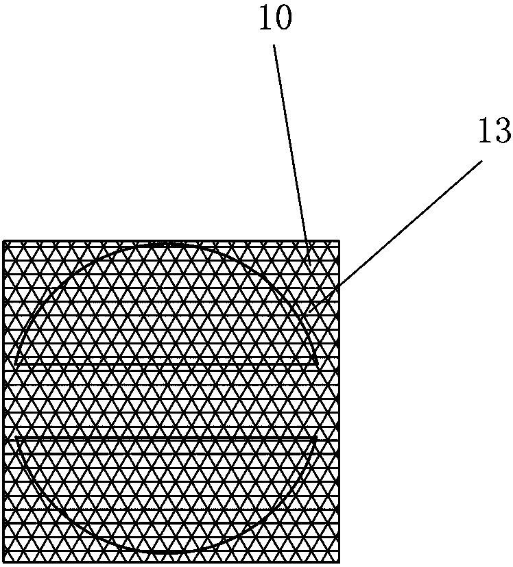
[0028] like image 3 , Figure 4As shown, the general structure of a frequency band compatible implementation system provided in this embodiment is the same as that of Embodiment 1, the difference is that, as another embodiment, in order to facilitate operation, the first short-circuit pad 10 and the second A stencil 13 is provided on the short-circuit pads 11 , and the stencil 13 has a perforated or non-perforated structure, and a layer of solder paste 14 is provided on the perforated stencil 13 .

Embodiment 3

[0030] like Figure 5 As shown, the general structure of a frequency band compatible implementation system provided in this embodiment is the same as that of Embodiment 1, the difference is that, as another embodiment, in order to facilitate processing, the first short-circuit pad 10 and The second short-circuit pad 11 is a circular pad, and a rectangular space 12 with a green window is provided in the middle.


PUM


Abstract

The invention discloses a system and a method for achieving frequency band compatibility. The system comprises a PCB and a frequency band compatible circuit, wherein the frequency band compatible circuit comprises a transceiver, a central processor, an antenna, an antenna switch, a first duplexer, a second duplexer, a single-pole double-throw switch and two short-circuit welding pads, wherein both ends of the transceiver are connected with two output ports of differential output signals of the single-pole double-throw switch, both ends of a first differential input end in the single-pole double-throw switch are connected with two output ends of the differential output signals of the single-pole double-throw switch separately through one of the independent short-circuit welding pads, two ports of the first differential input end in the single-pole double-throw switch are connected with the first duplexer, two ports of a second differential input end in the single-pole double-throw switch are connected with the second duplexer, output ends of the two duplexers are connected with the antenna through the antenna switch, and the central processor is connected with the single-pole double-throw switch. The system and the method achieve coexistence of two frequency bands truly, and ensure the RF performance.

Description

technical field [0001] The invention relates to a compatible method, in particular to a system and method for realizing frequency band compatibility. Background technique [0002] With the rapid development of modern communication technology, mobile communication has developed from the initial analog technology to the current 4G LTE era, with higher and higher data transmission rates, more and more adjustment systems and supported frequency bands. [0003] However, different countries or regions support different LTE frequency bands. The commonly used LTE frequency bands in Europe are band3, band7, and band20. The commonly used LTE frequency bands in South America are band4, band7, and band17. Some operators will use band28. Therefore, in order to meet the needs of different customers, frequency band compatibility becomes very necessary. However, the number of receiving ports at the transceiver end is limited, the PCB layout area is particularly tight, and the RF wiring is p...

Claims


Application Information

Patent Timeline
Patent Type & Authority Patents(China)
IPC IPC(8): H04B1/40H04L5/00H05K1/11
CPCH04B1/40H04L5/0005H05K1/111H05K2201/094
Inventor 李明英陈天赐常爱民林水明陈文伟
Owner NINGBO SAGEREAL COMM
Learn More