

Single-lens device for automatically detecting two-dimensional morphology and temperature of water substrate
An automatic detection and single-lens technology, applied in the direction of measuring devices, instruments, etc., can solve the problem of high cost and achieve the effect of cost reduction
- Summary
- Abstract
- Description
- Claims
- Application Information
AI Technical Summary
Problems solved by technology
Method used
Image

Examples
Embodiment 1
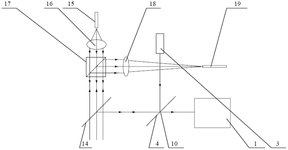
[0031] For ease of understanding, the attached image 3 The light path diagram of only one of the spots is given.
[0032] The single-lens type automatic detection device for the two-dimensional shape and temperature of the wafer base includes a single-lens type automatic detection device for the two-dimensional shape and temperature of the wafer base, a second light splitting element, and a device for detecting the temperature of the wafer base.
[0033] The single-lens type automatic detection device for the two-dimensional shape and temperature of the wafer substrate includes N PSDs, N beams of laser light and the first light splitting element. The N beams of laser light correspond one-to-one. The N beams of laser light are reflected by the first beam splitting element and then enter the second beam splitting element. After passing through the second beam splitting element, the incident light is formed. N incident points are formed, and the incident light is reflected by t...
Embodiment 2
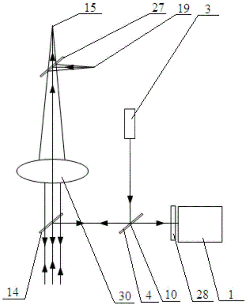
[0063] See attached Figure 4 The difference between the single-lens type automatic detection device for the two-dimensional shape and temperature of the wafer substrate provided by the second embodiment of the present invention and the first embodiment of the present invention is that the N-beam laser is controlled by an attached Figure 5 The multi-channel laser emitting device shown emits. The multi-path laser emitting device used in the single-lens type automatic detection of the two-dimensional shape and temperature of the wafer substrate provided by the present invention includes a multi-path beam splitting prism 26 and a laser 25, and the multi-path beam splitting prism 26 includes a plurality of beam splitting surfaces, multiple Parallel between the two beam splitting surfaces, the included angle α between the multiple beam splitting surfaces and the horizontal direction is 45° respectively, the centers of the multiple beam splitting surfaces are on the same straight l...
Embodiment 3
[0069] The difference between the single-lens type automatic detection of the two-dimensional shape and temperature of the wafer substrate provided by the third embodiment of the present invention and the first and second embodiments of the present invention is that the single-lens automatic detection of the wafer substrate provided by the third embodiment of the present invention The two-dimensional shape and temperature device can also include a light-passing device, which is arranged on the optical path where the incident light and the first reflected light beam pass through together, and the light-passing device is provided with N light-passing holes, and N light-passing holes There is one-to-one correspondence between the holes and the N beams of laser light, and reflectors 11 are arranged at intervals in the light-passing holes, which are used to reverse the direction of the corresponding passing beam by 90°, so that the corresponding PSD can be turned to another direction...
PUM
 Abstract
Description
Claims
Application Information