

NAND Flash fault tolerant system based on FPGA (Field Programmable Gate Array)
A fault-tolerant system and subsystem technology, applied in static memory, instruments, etc., can solve the problems that data cannot be read and written normally, invalid blocks cannot be erased, and Flash is scrapped, so as to solve the problem of bad block detection and management problems, overall performance and processing speed guarantees, and low-cost effects
- Summary
- Abstract
- Description
- Claims
- Application Information
AI Technical Summary
Problems solved by technology
Method used
Image

Examples
Embodiment Construction
[0021] The present invention will be further described below in conjunction with drawings and embodiments.
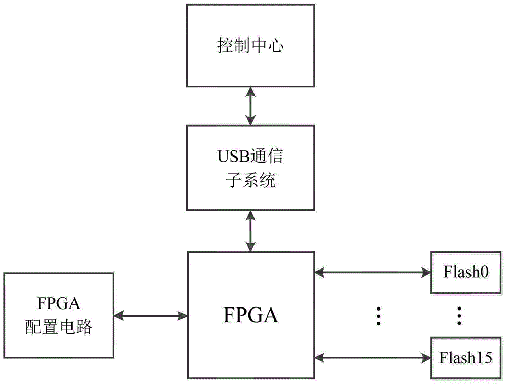
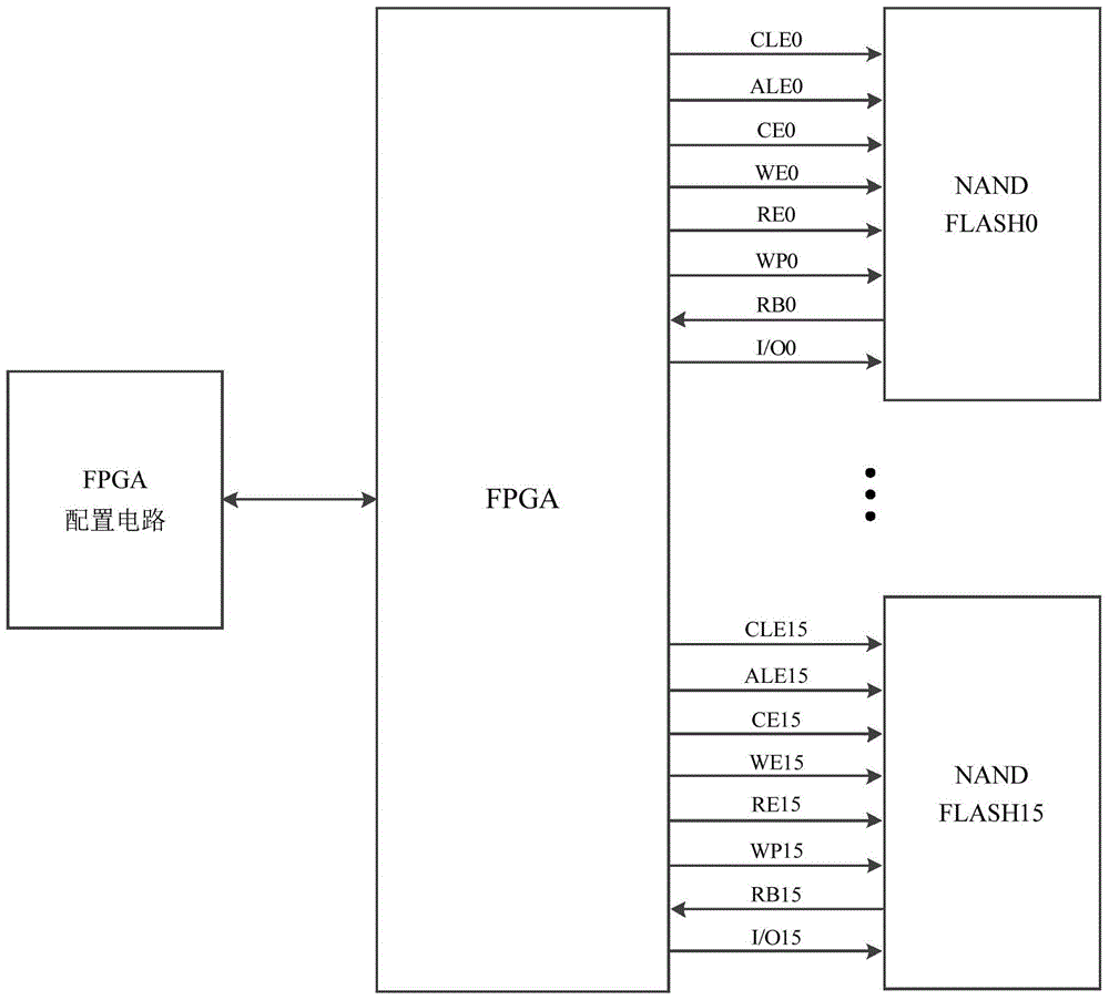
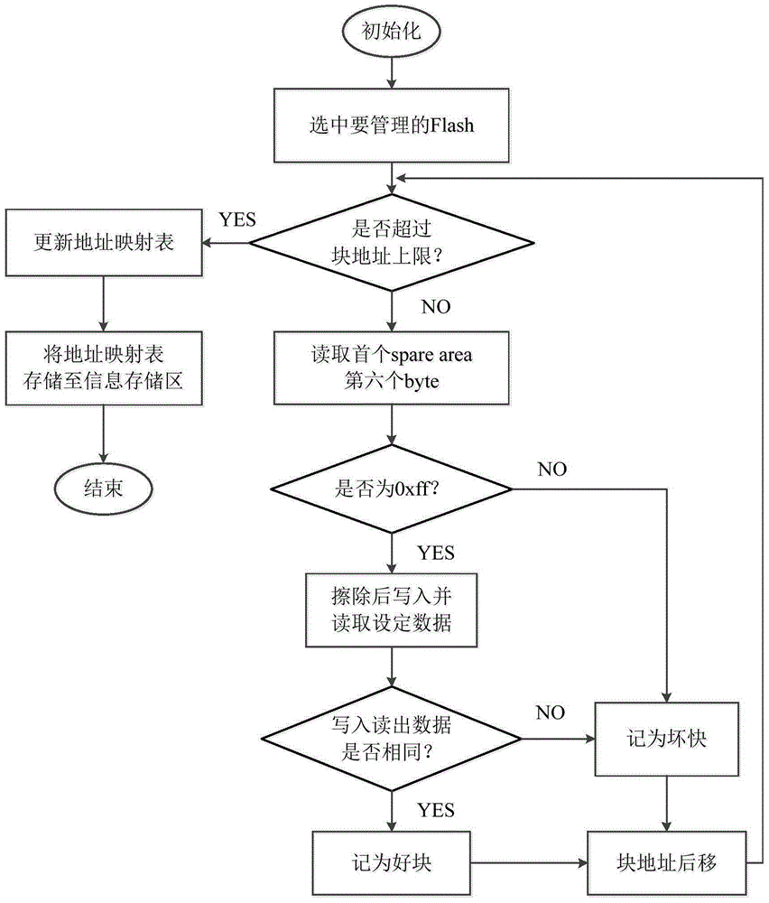
[0022] Such as figure 1 As shown, the FPGA-based NAND Flash fault-tolerant system proposed by the present invention includes a Flash bad block management subsystem, a USB communication subsystem and a host computer. The Flash bad block management subsystem is composed of FPGA and Flash array. It detects the factory bad blocks by querying the flag bits of the Flash in the sparearea, checks the return status of the read, write and erase operations, detects the damaged blocks, and records the addresses of all bad blocks. Divide the Flash into three logical areas, namely mapped good block area, bad block area, and information storage area, and establish an address mapping table to store in the information storage area. As the core controller, FPGA communicates with the host computer through the USB communication subsystem, and can receive control instructions and upload da...
PUM
 Abstract
Description
Claims
Application Information