Chip on film, flexible display panel and display device

A chip-on-chip and flexible display technology, which is applied in identification devices, static indicators, semiconductor/solid-state device components, etc., can solve problems such as poor binding between COF and flexible display panels, misalignment of input pads, etc., and achieve improvement Binding yield, avoiding misalignment, and increasing the effect of crimping area

Active Publication Date: 2016-06-29
BOE TECH GRP CO LTD
View PDF4 Cites 29 Cited by
  • Summary
  • Abstract
  • Description
  • Claims
  • Application Information

AI Technical Summary

Problems solved by technology

[0004] Both the vapor deposition process and the peeling process in the above manufacturing process will cause expansion of the flexible display panel, and, in the binding area of ​​the flexible display panel, the expansion of the middle area is smaller than the expansion of the two side areas. When the thin film (ChipOnFilm, COF) is bound to the flexible display panel, the output pad of the COF and the input pad in the binding area of ​​the flexible display panel will be misaligned, resulting in poor binding of the COF and the flexible display panel.

Method used


Image

  • Chip on film, flexible display panel and display device
  • Chip on film, flexible display panel and display device
  • Chip on film, flexible display panel and display device

Examples


example 1

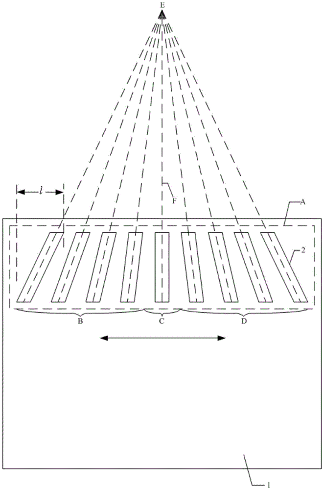
[0056] Example 1: The area where each row of input pads is located is divided into three areas: the first area, the second area and the third area.

[0057] In specific implementation, in the above flexible display panel provided by the embodiment of the present invention, since the second area is located in the center of the area where a row of input pads is located, the first area and the third area are respectively located on both sides of the second area, and the flexible The expansion of the middle area in the binding area of ​​the display panel less than that of the side areas results in a smaller spacing between adjacent input pads in the middle area than in the side areas, so , in order to increase the crimping area between the input pad in the binding area of ​​the flexible display panel and the output pad of the chip-on-chip film, and avoid misalignment between the output pad of the chip-on-film and the input pad in the binding area of ​​the flexible display panel To...

example 2

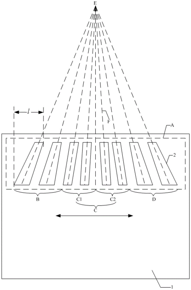
[0060] Example 2: The area where each row of input pads is located is divided into the first area, the second area and the third area, wherein the second area is divided into an even number of sub-areas, and the second area is divided into two sub-areas as an example. The area where each row of input pads is located is divided into four areas.

[0061] In specific implementation, in the above-mentioned flexible display panel provided by the embodiment of the present invention, the second area can be equally divided into M sub-areas, where M is an even number (that is, M=2, 4, 6...), figure 2 Taking the second area C equally divided into the first sub-area C1 and the second sub-area C2 as an example; since the first sub-area C1 and the second sub-area C2 are located in the center of the area where a row of input pads 2 is located, the first area B and the third area D are respectively located on both sides of the first sub-area C1 and the second sub-area C2, and the expansion ...

example 3

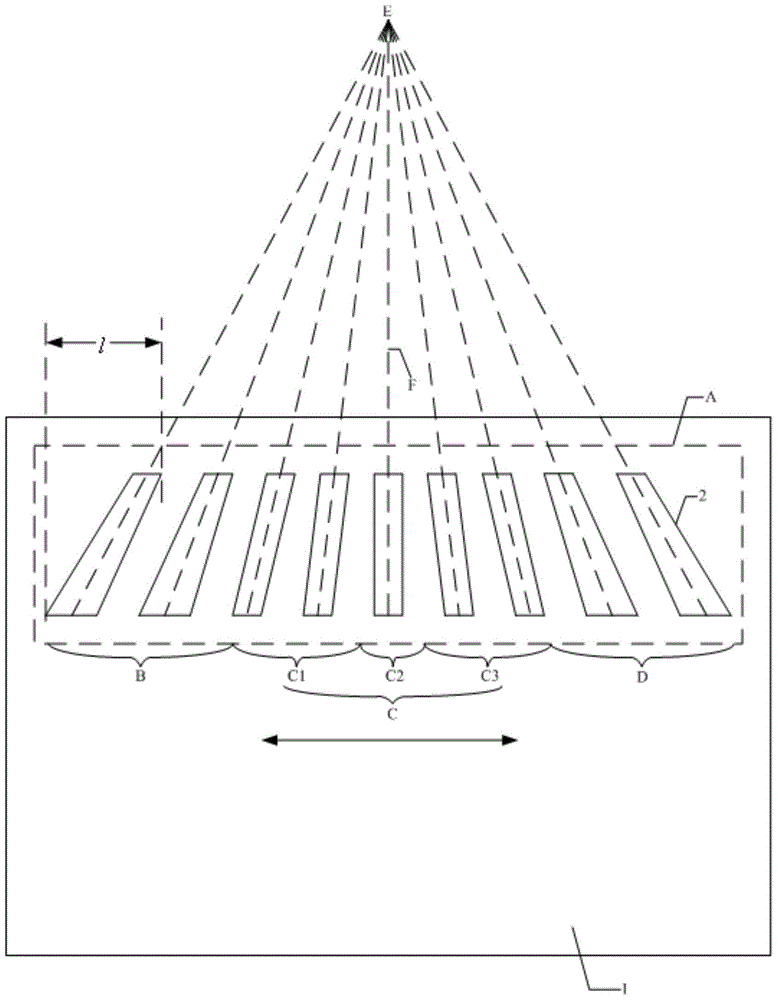
[0064] Example 3: The area where each row of input pads is located is divided into a first area, a second area and a third area, wherein the second area is divided into an odd number of sub-areas greater than 1, and the second area is divided into three sub-areas as For example, the area where each row of input pads is located is divided into five areas.

[0065] In specific implementation, in the above-mentioned flexible display panel provided by the embodiment of the present invention, the second area can be equally divided into N sub-areas, where N is an odd number greater than 1 (that is, N=3, 5, 7...), image 3 Taking the second area C equally divided into the first sub-area C1, the second sub-area C2 and the third sub-area C3 as an example; since the second sub-area C2 is located in the center of the second area C, the second area C is located at a The center of the area where a row of input pads 2 is located, that is, the second sub-area C2 is located in the center of t...


PUM


Abstract

The invention discloses a chip on film, a flexible display panel and a display device. When a swelling amount of a middle area in a binding area of the flexible display panel is smaller than swelling amounts of areas on both sides, input pad distances in the middle area are smaller than input pad distances in the areas on both sides. In the chip on film disclosed by the invention, output pads positioned in different areas are set into different shapes, namely, the output pads in the middle area are set into shapes to occupy small space while the output pads in the areas on both sides are set into shapes to occupy relatively large space, so that the chip on film can adapt to deformation at different positions in the binding area of the flexible display panel; a compression joint area between the chip on film and the binding area of the flexible display panel is increased; the problem of misalignment between the output pads of the chip on film and input pads in the binding area of the flexible display panel is solved; and a binding yield between the chip on film and the flexible display panel is increased.

Description

technical field [0001] The invention relates to the field of display technology, in particular to a chip-on-chip film, a flexible display panel and a display device. Background technique [0002] With the rapid development of display technology, flexible display panels have been favored by many users due to their advantages of thinness, light weight, drop resistance, bendability, and energy saving, and have become a recent research hotspot. [0003] The manufacturing process of the existing flexible display panel generally includes the following steps: first, coating polyimide (PI) film or polyethylene terephthalate (PET) film on rigid glass; Film or PET film is evaporated on the flexible substrate to form multiple flexible display panels; then, the formed multiple flexible display panels are peeled off from the rigid glass; finally, cut into multiple independent flexible display panels. [0004] Both the vapor deposition process and the peeling process in the above manufac...

Claims


Application Information

Patent Timeline
Patent Type & Authority Applications(China)
IPC IPC(8): H01L23/488
CPCH01L24/30H01L2224/3003H01L23/488H01L2224/06H01L27/1218H01L27/1244G09F9/301G09G3/20H01L21/77H01L23/528H01L24/01H01L27/12
Inventor 李红陈立强
Owner BOE TECH GRP CO LTD
Why Eureka
Try Eureka