High Speed Ge/Silicon Avalanche Photodiode
An avalanche photoelectric and diode technology, applied in circuits, electrical components, semiconductor devices, etc., can solve problems such as impact, increased capacitance, and increased RC time
- Summary
- Abstract
- Description
- Claims
- Application Information
AI Technical Summary
Problems solved by technology
Method used
Image

Examples
Embodiment Construction
[0016] The present invention provides various embodiments of novel germanium / silicon avalanche photodiode (Ge / Si APD) structures that address the aforementioned problems associated with existing Ge / Si APD designs.
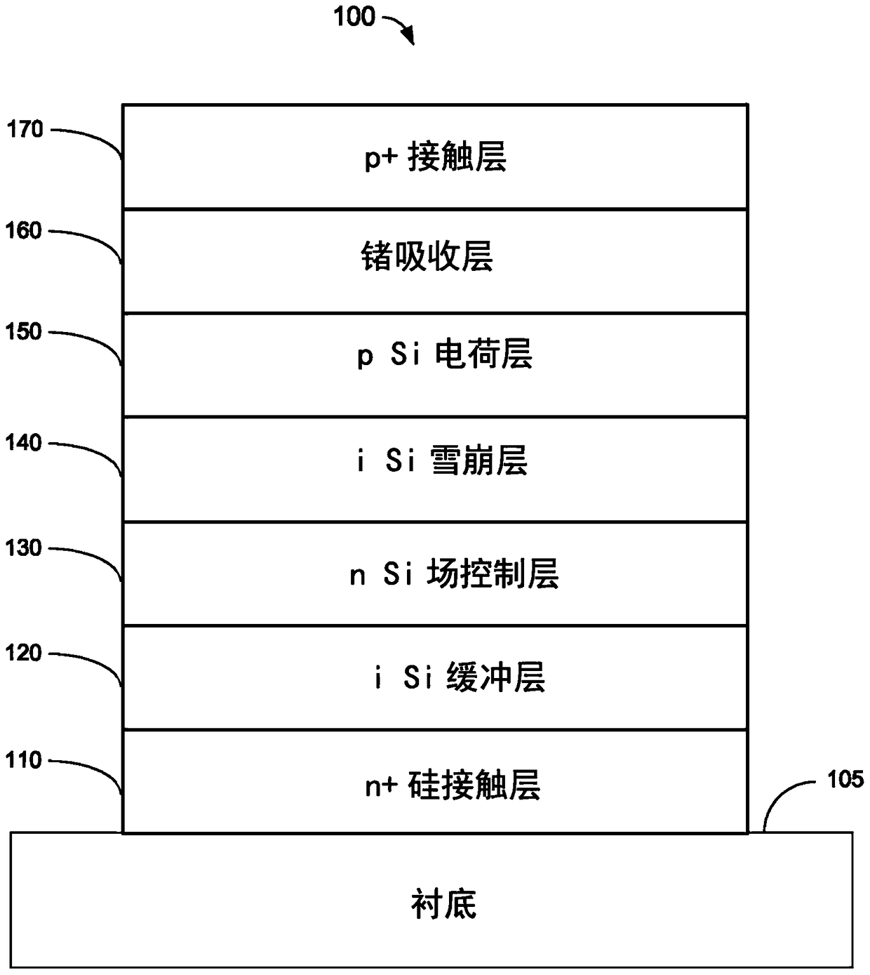
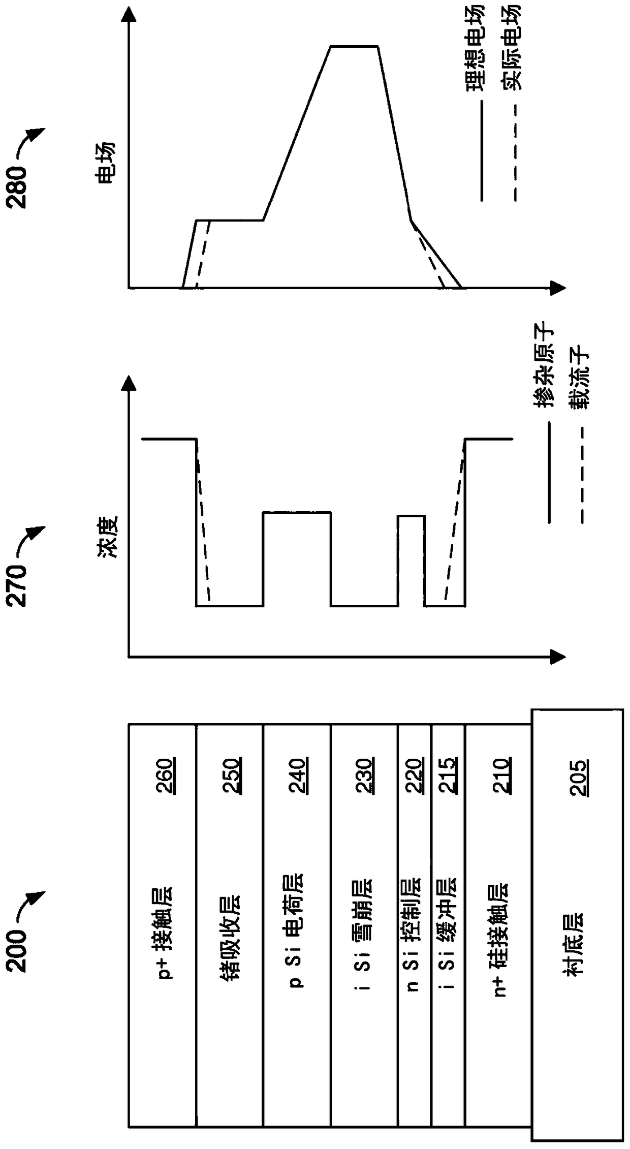
[0017] figure 1 A Ge / Si APD structure 100 is shown in accordance with one embodiment of the invention. refer to figure 1 , Ge / Si APD structure 100 may include substrate layer 105 , bottom contact layer 110 , buffer layer 120 , electric field control layer 130 , avalanche layer 140 , charge layer 150 , absorber layer 160 and top contact layer 170 . The substrate layer 105 may be prepared from a bulk silicon wafer or a silicon-on-insulator (SOI) wafer. The bottom contact layer 110 may be a heavily n-doped (n+) silicon contact layer. The buffer layer 120 may be an intrinsic silicon (i-Si) buffer layer. The electric field control layer 130 can be an n-doped silicon electric field control layer for controlling the electric field distribution in the avalanche layer...
PUM
 Abstract
Description
Claims
Application Information
 - R&D
- Intellectual Property
- Life Sciences
- Materials
- Tech Scout
- Unparalleled Data Quality
- Higher Quality Content
- 60% Fewer Hallucinations
Browse by: Latest US Patents, China's latest patents, Technical Efficacy Thesaurus, Application Domain, Technology Topic, Popular Technical Reports.
© 2025 PatSnap. All rights reserved.Legal|Privacy policy|Modern Slavery Act Transparency Statement|Sitemap|About US| Contact US: help@patsnap.com