

MOS tube parameter degradation detection circuit
A technology of MOS tube and parameter degradation, applied in the direction of measuring electricity, measuring electrical variables, measuring devices, etc., can solve problems such as MOS tube parameter degradation
- Summary
- Abstract
- Description
- Claims
- Application Information
AI Technical Summary
Problems solved by technology
Method used
Image

Examples
Embodiment Construction
[0017] In order to make the object, technical solution and advantages of the present invention clearer, the present invention will be further described in detail below in conjunction with the accompanying drawings and embodiments. It should be understood that the specific embodiments described here are only used to explain the present invention, and do not limit the protection scope of the present invention.
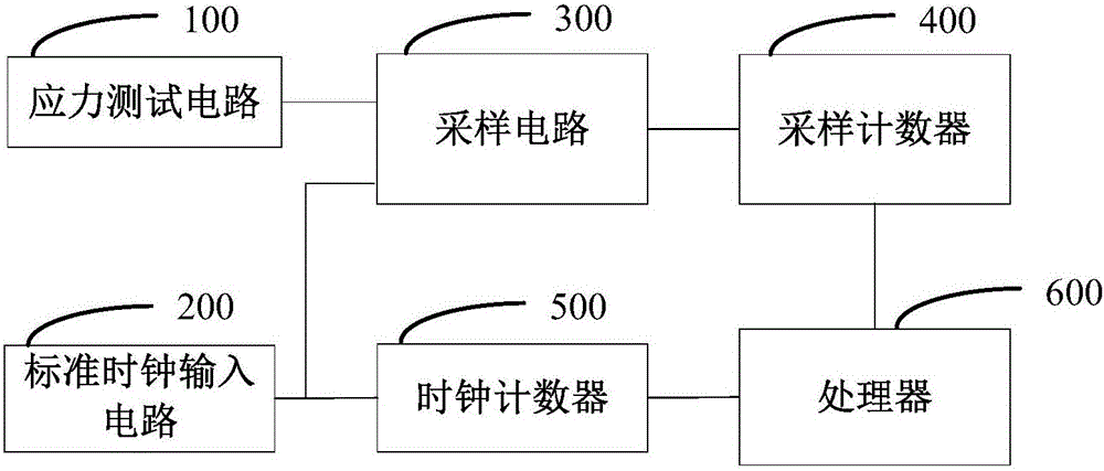
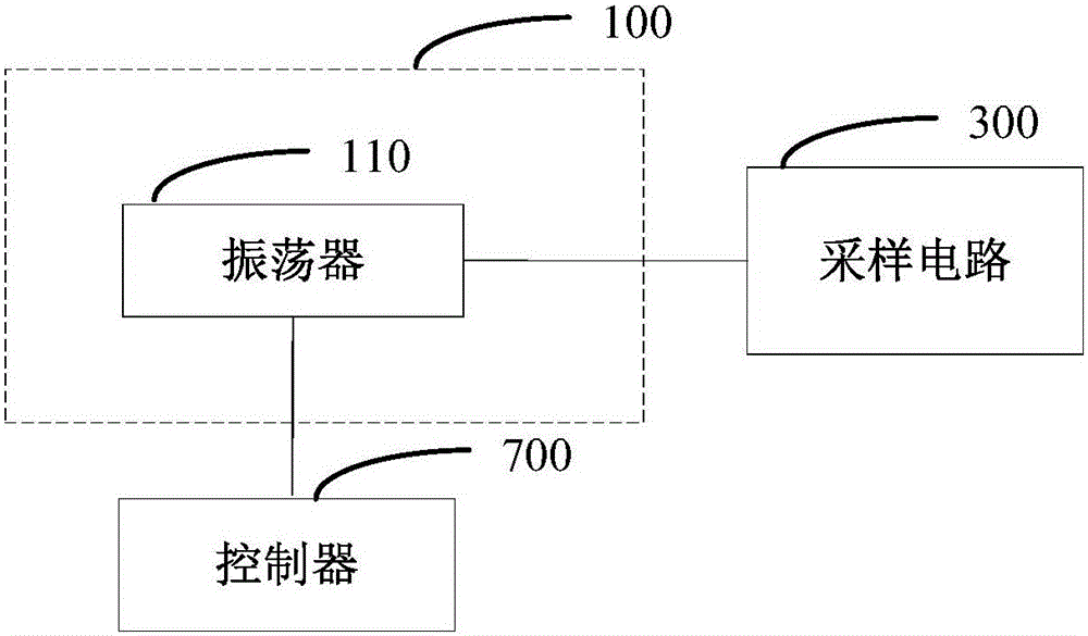
[0018] see figure 1 Shown is an embodiment of the detection circuit for MOS tube parameter degradation of the present invention. The detection circuit of the MOS transistor parameter degradation in this embodiment includes a stress test circuit 100, a standard clock input circuit 200, a sampling circuit 300, a sampling counter 400, a clock counter 500 and a processor 600;
[0019] Stress test circuit 100, standard clock input circuit 200 are connected with sampling circuit 300 respectively, and sampling circuit 300 is connected with sampling counter 400, and sampling co...
PUM
 Abstract
Description
Claims
Application Information