Multi-core planar optical waveguide structure and coupling structure thereof

A planar optical waveguide and coupling structure technology, applied in the field of optical waveguide coupling, can solve the problems of high packaging cost, complex process, and difficulty in large-scale integration, and achieve the requirements of improving alignment tolerance, reducing cost, and reducing process accuracy Effect

Active Publication Date: 2016-07-13
WUHAN TELECOMM DEVICES
View PDF6 Cites 4 Cited by
  • Summary
  • Abstract
  • Description
  • Claims
  • Application Information

AI Technical Summary

Problems solved by technology

[0002] The current mainstream 40G / 100G optical modules are basically based on free space coupling technology such as prisms, lenses, optical filters, etc., which are characterized by complex processes, active alignment with light, high packaging costs, and large-scale integration are very difficult

Method used


Image

  • Multi-core planar optical waveguide structure and coupling structure thereof
  • Multi-core planar optical waveguide structure and coupling structure thereof
  • Multi-core planar optical waveguide structure and coupling structure thereof

Examples


Embodiment 1

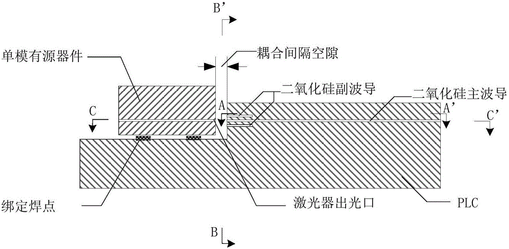
[0043] Embodiment 1 of the present invention provides a multi-core planar optical waveguide structure, such as figure 1 As shown, the multi-core planar optical waveguide structure includes:

[0044] The planar optical waveguide includes a silicon dioxide main waveguide for transmitting optical signals, and a secondary waveguide for assisting light entering;

[0045] The secondary waveguide includes one or more silica secondary waveguides, and the silica secondary waveguide is arranged according to a preset center distance from the silica main waveguide.

[0046] Wherein, the center distance is used to ensure that the one or more secondary silica waveguides and the main silica waveguide produce sufficient coupling effect on the light receiving surface.

[0047] The planar optical waveguide structure including one or more silica secondary waveguides proposed in the embodiments of the present invention can complete the passive alignment and direct coupling of the laser to the PL...

Embodiment 2

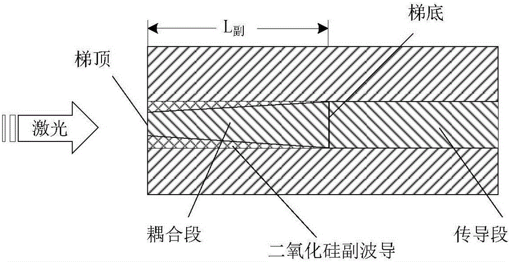
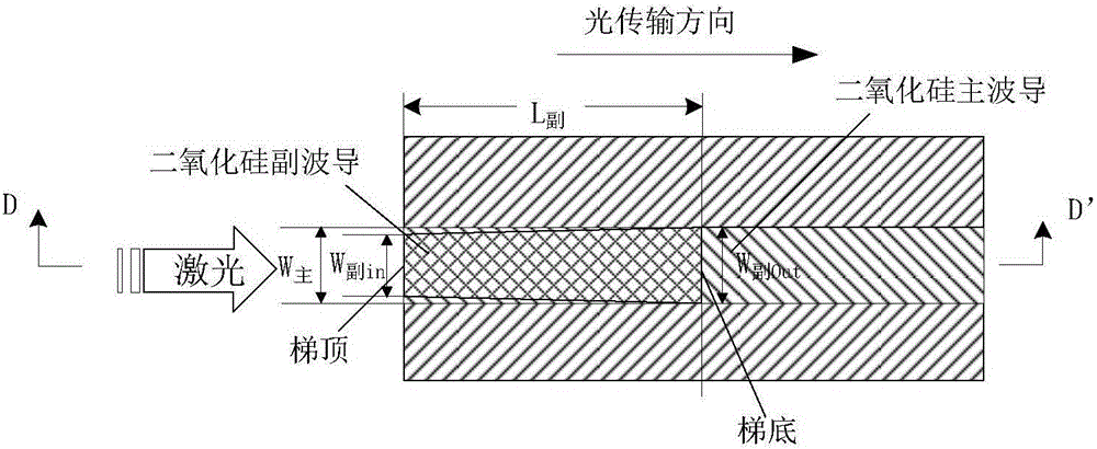
[0050] Based on the multi-core planar optical waveguide structure described in Embodiment 1, Embodiment 2 of the present invention specifically describes the composition of one of the optional silica secondary waveguides, as image 3 , Figure 4 and Figure 5 Shown:

[0051] The planar optical waveguide includes a silicon dioxide main waveguide for transmitting optical signals, and a secondary waveguide for assisting light entering;

[0052] The secondary waveguide specifically includes two sub-sub-waveguides, wherein the first sub-sub-waveguide is located on the upper side of the silica main waveguide, the second sub-sub-waveguide is located on the lower side of the silica main waveguide, and the two sub-sub-waveguides are located on the lower side of the silica main waveguide. The silicon oxide secondary waveguide and the silicon dioxide main waveguide are arranged according to a preset center distance.

[0053] Wherein, the center distance is used to ensure that the one ...

Embodiment 3

[0068] Based on the multi-core planar optical waveguide structure described in Embodiment 1, Embodiment 3 of the present invention specifically describes the composition of one of the optional silica secondary waveguides, as Figure 7 , Figure 8 and Figure 9 Shown:

[0069] The planar optical waveguide includes a silicon dioxide main waveguide for transmitting optical signals, and a secondary waveguide for assisting light entering;

[0070] The sub-waveguides specifically include eight sub-sub-waveguides, wherein the first sub-sub-waveguide 01 is located on the upper side of the silica main waveguide; the second sub-sub-waveguide 02 is located on the lower side of the silica main waveguide; The third sub-waveguide 03 is located on the left side of the silica main waveguide; the fourth sub-sub-waveguide 04 is located on the right side of the silica main waveguide; the fifth sub-sub-waveguide 05 is located on the side of the silica main waveguide The upper left side, and is...


PUM


Abstract

The invention relates to the technical field of optical waveguide coupling and provides a multi-core planar optical waveguide structure and a coupling structure thereof. The multi-core planar optical waveguide structure comprises a main silicon dioxide waveguide for transmitting optical signals and an auxiliary waveguide for assisting light incidence, wherein the auxiliary waveguide comprises one or more auxiliary silicon dioxide waveguide bodies, and the auxiliary silicon dioxide waveguide bodies and the main silicon dioxide waveguide are arranged according to present central distances. The planar optical waveguide structure including one or more auxiliary silicon dioxide waveguide bodies can complete passive light alignment and direct coupling from a laser device to a PLC. Compared with the prior art, the alignment tolerance can be improved. Based on the improvement of the alignment tolerance, the requirement for process precision in an automatic device can be further reduced, the time for light alignment and welding can be shortened, the defective percentage is further reduced, and accordingly the purpose of reducing the costs is achieved.

Description

【Technical field】 [0001] The invention relates to the technical field of optical waveguide coupling, in particular to a multi-core planar optical waveguide structure and its coupling structure. 【Background technique】 [0002] The current mainstream 40G / 100G optical modules are basically based on free space coupling technology such as prisms, lenses, optical filters, etc., which are characterized by complex processes, active alignment of light, high packaging costs, and large-scale integration are very difficult. [0003] On the other hand, photonic integration technology generally refers to active devices (lasers, detectors, optical amplifiers, optical modulators, etc.) ) integration to realize single-chip multi-functional optical device technology. Photonic integration technology is considered to be a powerful optical module technology in the near future and even in the future, especially in short-distance optical interconnection applications such as data centers. However...

Claims


Application Information

Patent Timeline
Patent Type & Authority Applications(China)
IPC IPC(8): G02B6/42
CPCG02B6/4228G02B6/4296
Inventor 陈奔梁雪瑞朱虎胡百泉张玓刘成刚周日凯付永安孙莉萍马卫东余向红
Owner WUHAN TELECOMM DEVICES
Why Eureka
Try Eureka