

Semiconductor LED and its preparing process
A technology of light emitting diodes and semiconductors, which is applied to semiconductor devices, electrical components, circuits, etc., can solve problems such as reducing light extraction efficiency, and achieve the effects of improving light extraction efficiency, improving light extraction efficiency, and optimizing design and processing.
- Summary
- Abstract
- Description
- Claims
- Application Information
AI Technical Summary
Problems solved by technology
Method used
Image

Examples
Embodiment 1
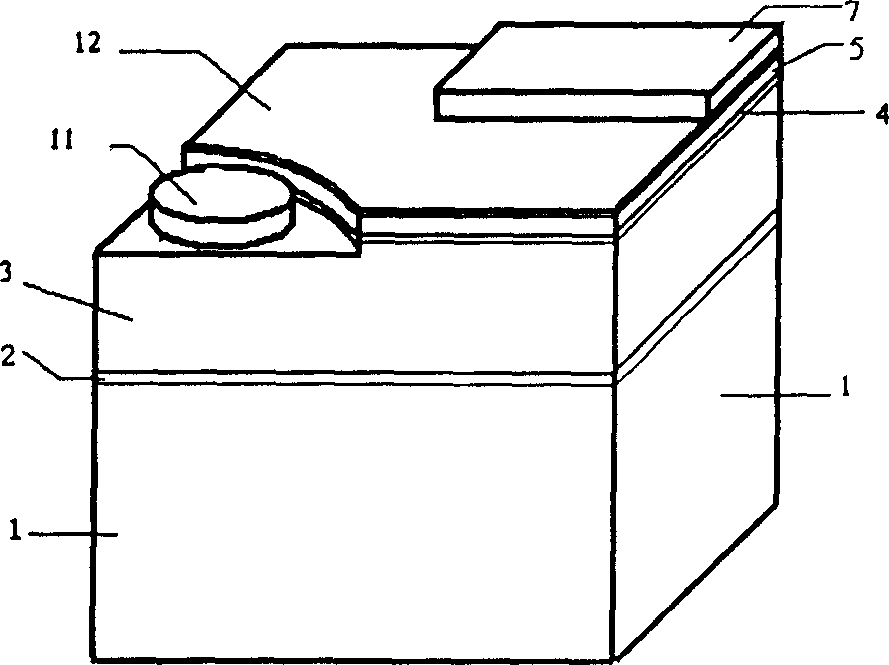
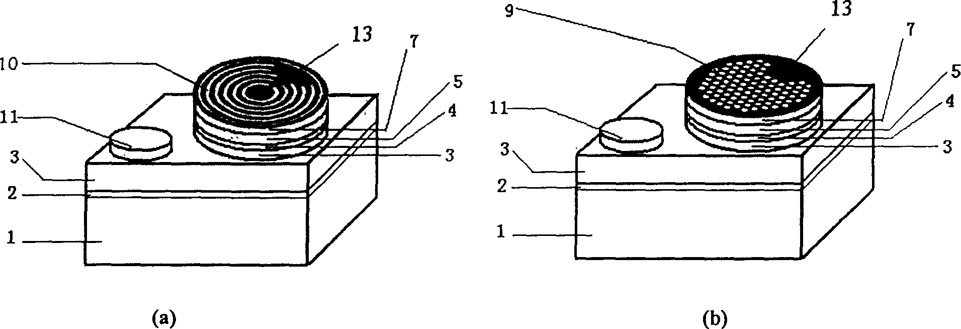
[0093] Honeycomb and concentric ring-type InGaN-based quantum well blue light-emitting diodes
[0094] 1. Using metal oxide chemical vapor deposition (MOCVD) equipment to grow InGaN multiple quantum well (MQW) epitaxial wafers, the hierarchical structure of the epitaxial wafers is:
[0095] P-GaN (thickness d=50-300nm, carrier concentration p=3-5×10 17 cm -3 ) / P-AlGaN (aluminum gallium nitrogen) (d=5-20nm, p=1-3×10 17 cm -3 ) / 3 quantum well [In x Ga 1-x N(indium composition x=0.18-0.25, d=20-30nm) / GaN(d=70-100nm)]QW / n-GaN(d=2000-3000nm, carrier concentration n=2×10 18 cm -3 ) / GaN buffer layer (d=25-30m) / sapphire substrate;
[0096] 2. Deposit p-type ohmic contact double-layer metal film gold (5-500 nm) / nickel (5-40 nm) by DC sputtering technology;
[0097] 3. Formed on the sample by ordinary photolithography technology Figure 4 the figure of (a) or (b);
[0098] 4. Using photoresist as a mask, argon (Ar) ion beam etching and boron trichloride (BCl) 3 ) reactive ion...
Embodiment 2
[0102] Honeycomb and Concentric Ring InGaAlP Quantum Well Red Light Emitting Diodes
[0103] 1. Using MOCVD InGaAlP quantum well (QW) epitaxial wafer;
[0104] 2. Deposit p-type ohmic contact double-layer metal film gold (100-500 nanometers) / chromium (20-40 nanometers) by vacuum thermal evaporation technology, and carry out in-situ alloying (400-450 ° C, 2 -5 minutes);
[0105] 3. Use ordinary photolithography technology to form a layout on the sample Figure 4 the figure of (a) or (b);
[0106] 4. Using photoresist as a mask, Ar ion beam etching is carried out successively, and the total etching depth reaches the n-type region;
[0107] 5. Vacuum thermal evaporation and alloying of the n-type ohmic contact alloy film of gold-germanium-nickel (AuGeNi) on the back (400-450°C, 2-5 minutes).
Embodiment 3
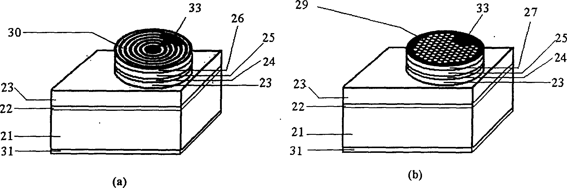
[0109] Preparation steps of FIB concentric ring-type InGaN-based quantum well blue light-emitting diode:
[0110] 1. Adopt MOCVD equipment to grow InGaN multiple quantum well (MQW) epitaxial wafer (same as embodiment 1);
[0111] 2. With embodiment 1 step 2;
[0112] 3. Using ordinary photolithography technology to form a plate on the epitaxial wafer Figure 4 the graphic of (d);
[0113] 4. Using photoresist as a mask, perform BCl 3 Reactive ion etching, the total etching depth reaches the n-type region;
[0114] 5. Version Figure 4 (c) performing photolithographic overlay;
[0115] 6. Deposition of n-type ohmic contact bilayer metal film gold (5-500 nm) / titanium (5-40 nm) by DC sputtering and lift-off technology
[0116] 7. Rapid annealing in a nitrogen atmosphere to form an ohmic contact (450-500°C, 2-5 minutes);
[0117] 8. Press the plate on the p-zone round table Figure 4 (a) or 4(b) perform FIB etching, and the etching depth reaches the n-type region.
PUM
| Property | Measurement | Unit |
|---|---|---|
| Thickness | aaaaa | aaaaa |
Abstract
Description
Claims
Application Information