Light emitting diode package and fabricating method thereof

a technology of light-emitting diodes and packaging, which is applied in the direction of semiconductor devices, semiconductor/solid-state device details, electrical devices, etc., can solve the problem of distorted geometry of light emitted from conventional leds

Inactive Publication Date: 2007-08-23
NOVALITE OPTRONICS CORP
View PDF5 Cites 50 Cited by
  • Summary
  • Abstract
  • Description
  • Claims
  • Application Information

AI Technical Summary

Benefits of technology

[0008]An object of the present invention is to provide an LED package. An ESD protector is buried within the package housing, so that the ESD protector will not affect the light-emitting intensity as well as the light shape of the LED package.
[0009]Another object of the present invention is to provide a fabricating method of an LED package, so as to bury the ESD protector inside the package housing, thereby improving the light-emitting intensity of the LED package.
[0023]In one embodiment of the present invention, the above-mentioned LED further includes a Phosphor doped encapsulant, which can encapsulate the LED chip and the carrier exposed by the chip-accommodating space.

Problems solved by technology

Also, the geometry of the light emitted from the conventional LED could be distorted due to the as-centered position of the Diode.

Method used


Image

  • Light emitting diode package and fabricating method thereof
  • Light emitting diode package and fabricating method thereof
  • Light emitting diode package and fabricating method thereof

Examples


first embodiment

The First Embodiment

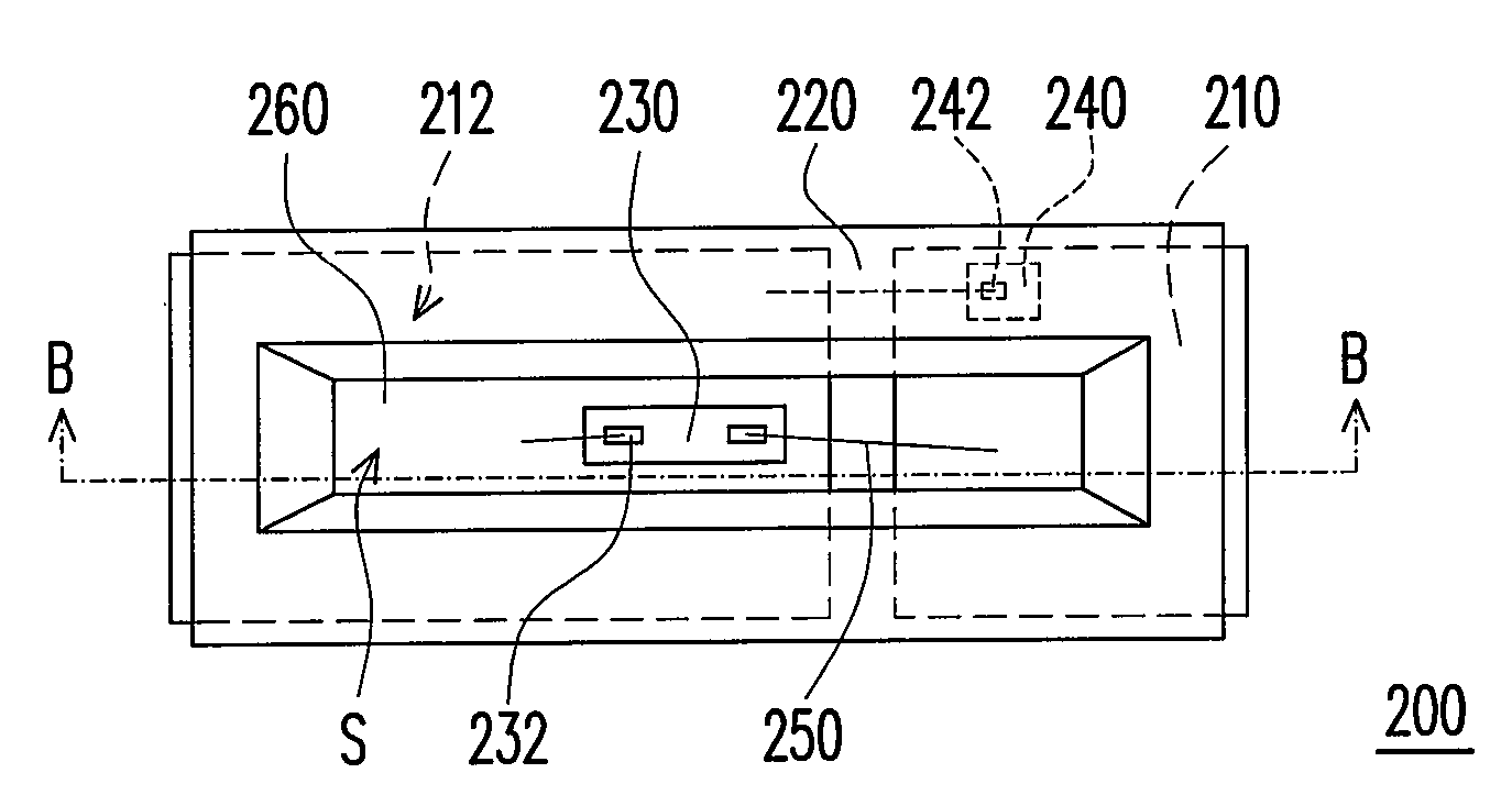
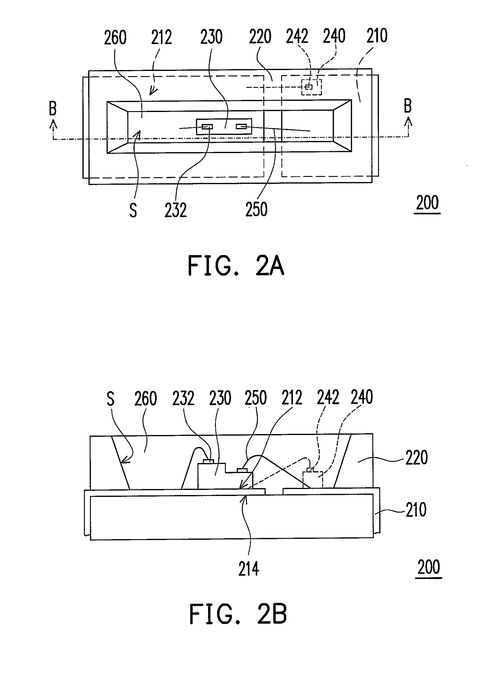
[0046]FIG. 2A shows a schematic top view of an LED package according to the first embodiment of the present invention. FIG. 2B shows a schematic sectional view of the LED package in FIG. 2A along Line B-B. Referring to FIGS. 2A and 2B at the same time, the LED package 200 of the first embodiment includes a carrier 210 (for example, a Lead Frame), a package housing 220 (the material thereof can be plastic, metal, or metal oxide), an LED chip 230, and an ESD protector 240. The package housing 220 encapsulates a part of the carrier 210 to form a chip-accommodating space S on the carrier 210. The LED chip 230 disposed on the carrier 210 and located in the chip-accommodating space S is electrically connected to the carrier 210. Furthermore, the ESD protector 240 disposed on the carrier 210 and encapsulated by the package housing 220 is electrically connected to the carrier 210.

[0047]In one embodiment of the present invention, the ESD protector 240 can be a one-directi...

second embodiment

The Second Embodiment

[0059]FIG. 5A shows a schematic top view of an LED package according to the second embodiment of the present invention. FIG. 5B shows a schematic sectional view of the LED package in FIG. 5A along Line C-C. Referring to FIGS. 2A, 2B, 5A, and 5B at the same time, the major difference between the LED package 300 of the second embodiment and the LED package 200 of the first embodiment is that the LED package 300 further includes a plurality of bumps 370. The ESD protector 340 can be electrically connected to the carrier 310 through the bumps 370, and the package housing 320 encapsulates the bumps 370. In other words, the ESD protector 340 is disposed on the carrier 310 and electrically connected to the carrier 310 via flip chip bonding technology.

[0060]It should be illustrated that, in the second embodiment, the LED chip 330 and the ESD protector 340 of the LED package 300 are electrically connected to the carrier 310 in different ways, and the two electrical conne...

third embodiment

The Third Embodiment

[0061]FIG. 6 shows a schematic sectional view of an LED package according to the third embodiment of the present invention. Referring to FIGS. 2A, 2B, and 6, the difference between the LED package 400 of the third embodiment and the LED package 200 of the first embodiment is that the LED chip 430 and the ESD protector 440 are, for example, respectively disposed on the two opposite surfaces 412 and 414 of the carrier 410.

[0062]In view of the above, the LED package and the fabricating method thereof according to the present invention have at least the following advantages.

[0063]For the LED package and the fabricating method thereof according to the present invention, the ESD protector can be encapsulated by the package housing, so when the LED chip is driven by the current to emit light, the non-transparent ESD protector will not absorb the light emitted by the LED chip, and thereby the light-emitting intensity of the LED package will not be affected.

[0064]Since th...


PUM


Abstract

A Light Emitting Diode (LED) package including a carrier, a package housing, an LED chip, and an electrostatic discharge protector (ESD protector) is provided. The package housing encapsulates a part of the carrier so as to provide a chip-accommodating space on the carrier. The LED chip disposed on the carrier and located in the chip-accommodating space is electrically connected to the carrier. The ESD protector disposed on the carrier and encapsulated by the package housing is electrically connected to the carrier. The LED package has excellent light-emitting intensity, since the light emitted from the LED chip is not absorbed by the ESD protector encapsulated by the package housing. Additionally, a fabricating method of the LED package is also provided.

Description

CROSS-REFERENCE TO RELATED APPLICATION[0001]This application claims the priority benefit of Taiwan application serial no. 95106043, filed on Feb. 23, 2006. All disclosure of the Taiwan application is incorporated herein by reference.BACKGROUND OF THE INVENTION[0002]1. Field of Invention[0003]The present invention relates to a package structure and a fabricating method thereof. More particularly, the present invention relates to a light emitting diode package (LED package) having a hidden ESD protector and a fabricating method thereof.[0004]2. Description of Related Art[0005]Since the LED has such advantages as long service life, small volume, high shock resistance, low heat output, and low power consumption, it has been widely utilized in indicators or light sources for household appliances and various instruments. In recent years, the LED has been developed towards multicolor and high brightness; therefore, its application scope has been expanded to large outdoor display boards, tr...

Claims


Application Information

Patent Timeline
Patent Type & Authority Applications(United States)
IPC IPC(8): H01L23/06H01L33/50H01L33/60H01L33/62
CPCH01L25/167H01L2224/48227H01L2224/48247H01L2224/49107H01L2224/48091H01L2924/00014
Inventor LAI, KOU-RUEHYANG, GWO-SHIIHO, KUNG-CHITSAI, HU-CHENWANG, WEN-CHUAN
Owner NOVALITE OPTRONICS CORP
Why Eureka
Try Eureka