Manufacturing method of light emitting device

a manufacturing method and light-emitting technology, applied in semiconductor devices, lasers, semiconductor lasers, etc., can solve problems such as difficulty in achieving larger luminous intensity, and achieve the effects of reducing luminous intensity, improving luminous intensity, and reducing luminous intensity

Inactive Publication Date: 2000-12-19
SANYO ELECTRIC CO LTD
View PDF15 Cites 51 Cited by
  • Summary
  • Abstract
  • Description
  • Claims
  • Application Information

AI Technical Summary

Benefits of technology

Particularly, it is preferable that the Al composition ratio u of the cap layer is approximately 0.1 or smaller. It is more preferable that the cap layer is composed of GaN. In this case, since the cap layer is formed of a GaN layer, elimination of constituent elements such as indium from the active layer is suppressed, thus providing significantly larger luminous intensity.
Particularly, it is preferable that the cap layer is an undoped layer. In this case, there is almost no possibility a of diffusion of undesirable impurities from the cap layer side to the active layer side. This sufficiently suppresses deterioration of luminous intensity due to undesirable impurity diffusion.
It is preferred that the cap layer has a thickness of approximately not smaller than 200 .ANG. and approximately not larger than 400 .ANG.. This enables remarkable improvement of t...

Problems solved by technology

This causes difficulty in achieving larger ...

Method used


Image

  • Manufacturing method of light emitting device
  • Manufacturing method of light emitting device
  • Manufacturing method of light emitting device

Examples


first embodiment

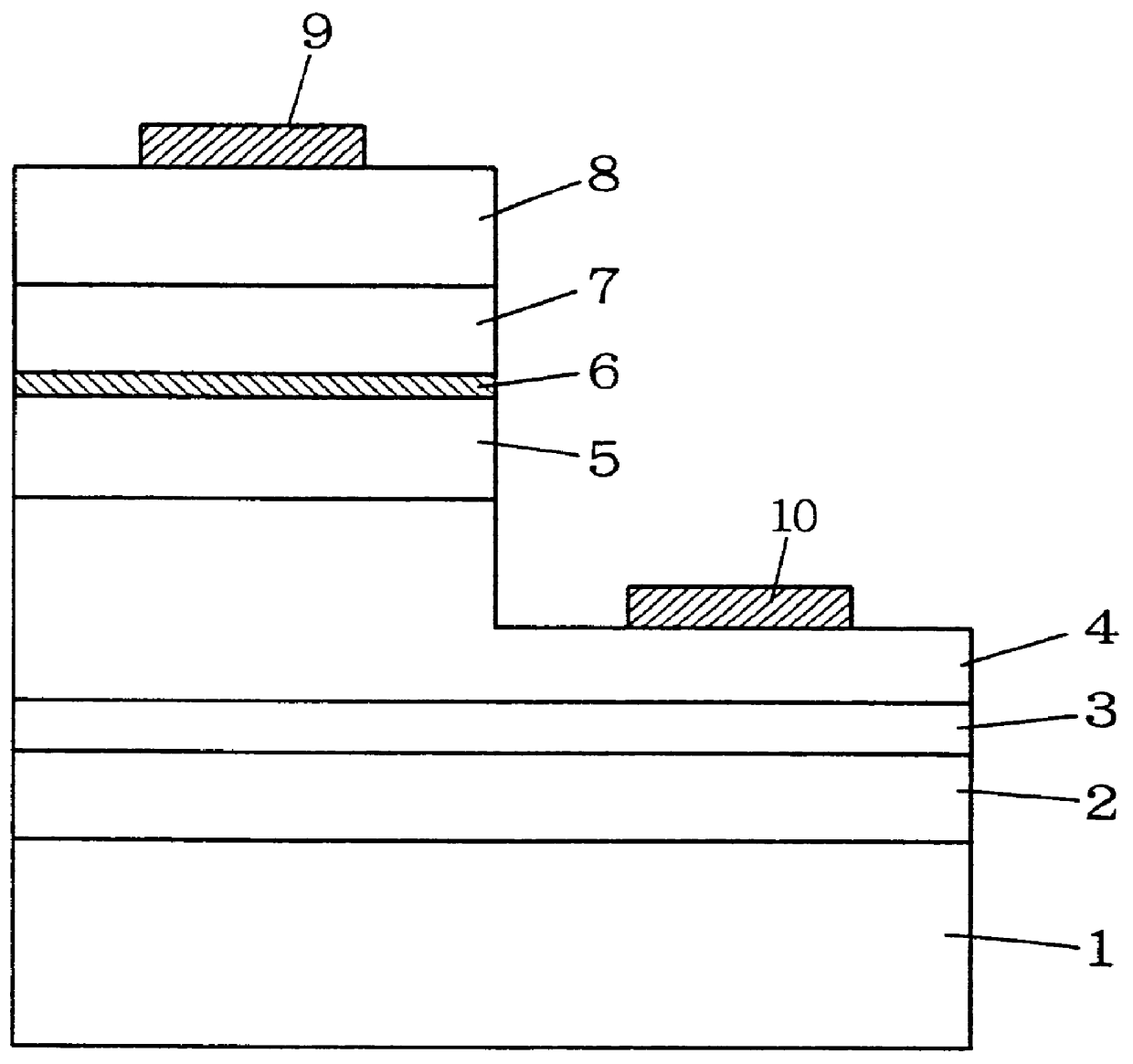
A light emitting diode composed of III-V group nitride system semiconductors according to the present invention will now be described in detail referring to FIG. 1.

In FIG. 1, formed in order on a sapphire insulating substrate 1 are a 110-.ANG.-thick undoped Al.sub.x Ga.sub.1-x N (x=0.5) buffer layer 2, a 0.2-.mu.m-thick undoped GaN underlayer 3, a 4-.mu.m-thick Si-doped n-type GaN contact layer 4 also serving as an n-type cladding layer, and a 0.2-.mu.m-thick Zn- and Si-doped In.sub.q Ga.sub.1-q N (q=0.05) active layer 5. Formed in order on the InGaN active layer 5 are a 200-.ANG.-thick undoped GaN cap layer 6 for preventing crystal deterioration of the active layer 5, a 0.15-.mu.m-thick Mg-doped p-type Al.sub.z Ga.sub.1-z N (z=0.2) cladding layer 7, and a 0.3-.mu.m-thick Mg-doped p-type GaN contact layer 8.

The part from the p-type GaN contact layer 8 to a certain position in the n-type GaN contact layer 4 is removed, so that the n-type GaN contact layer 4 is exposed. A p electrode ...

second embodiment

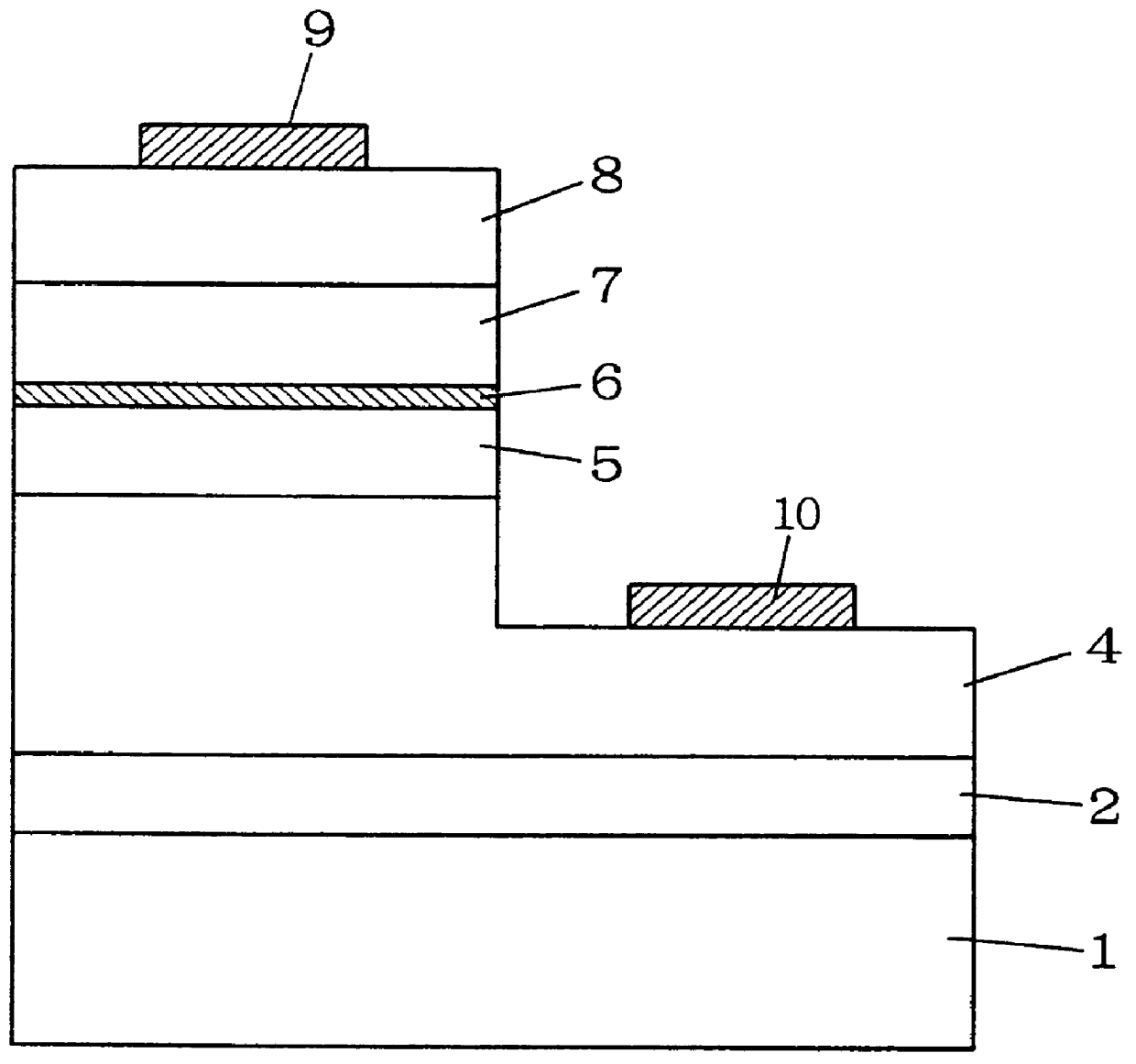
Next, a light emitting diode formed of III-V group nitride system semiconductors in the present invention will be described.

This embodiment differs from the first embodiment in that it uses a 200-.ANG.-thick undoped Al.sub.u Ga.sub.1-u N layer as the cap layer 6 in place of the undoped GaN layer. The value of u is approximately 0.1 and 0.2. This Al.sub.u Ga.sub.1-u N layer, too, is formed by MOCVD at the same temperature as the growth temperature for the active layer 5, at 860.degree. C. in this embodiment. H.sub.2 and N.sub.2 are used as carrier gas and ammonia, trimethylgallium (TMG) and trimethylaluminum (TMA) are used as material gas. Triethylgallium (TEG) may be used instead of trimethylgallium (TMG).

It was seen that the light emitting diode of this embodiment also provides remarkably larger luminous intensity than a light emitting diode having no cap layer 6.

However, as compared with the 200-.ANG.-thick undoped GaN cap layer 6 in the first embodiment regarded as providing a lu...

third embodiment

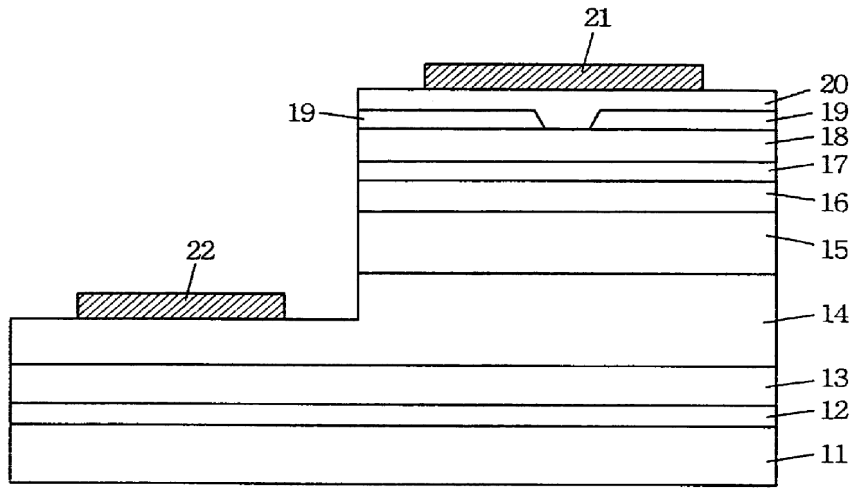
Next, a light emitting diode composed of III-V group nitride system semiconductors in the invention will be described referring to FIG. 2.

This embodiment differs from the first embodiment in that it uses no GaN underlayer 3, whose manufacturing method is the same as that in the first embodiment except that it excludes the process step for forming the GaN underlayer 3.

While the light emitting diode of this embodiment provides lower yield than the light emitting diode of the first embodiment, it achieves larger luminous intensity than a light emitting diode having no cap layer 6.

Although the light emitting diodes of the above-described embodiments have the active layer 5 on the n-type contact layer 4, an n-type AlGaN cladding layer may be provided between the n-type contact layer 4 and the active layer 5. An n-type AlGaN cladding layer and an n-type InGaN layer may be provided between the n-type contact layer 4 and the active layer 5.

The aforementioned embodiments use an active layer ...


PUM


Abstract

A method of manufacturing a light emitting device, including the steps of: forming an active layer composed of a compound semiconductor containing indium by a vapor phase growth method; and forming a cap layer composed of a compound semiconductor on said active layer by a vapor phase growth method at a growth temperature approximately equal to or lower than a growth temperature for said active layer.

Description

BACKGROUND OF THE INVENTION1. Field of the InventionThe present invention relates to a light emitting device and a manufacturing method thereof.2. Description of the Background ArtLight emitting devices such as light emitting diodes and semiconductor laser devices which are formed of III-V group nitride system semiconductors such as GaN, AlGaN, InGaN and InAlGaN are receiving a great deal of attention because they are capable of, by direct transition, light emission in the yellow to ultraviolet region, especially in the blue region, with large luminous intensity.FIG. 8 is a schematic cross-sectional view showing a conventional light emitting diode composed of III-V group nitride system semiconductors.In FIG. 8, formed in order on a sapphire substrate 101 are a GaN buffer layer 102, an n-type GaN contact layer 103 also serving as an n-type cladding layer, an InGaN active layer 104, a p-type AlGaN cladding layer 105, and a p-type GaN contact layer 106. A p electrode 107 is formed on t...

Claims


Application Information

Patent Timeline
IPC IPC(8): H01L33/00H01S5/323H01S5/00H01L33/06H01L33/12H01L33/32H01L33/34H01S5/343
CPCH01L33/007H01L33/32H01L33/02H01S5/0213H01S5/221H01S5/32341H01S2301/173H01S2304/04H01S5/2231H01S5/321H01S5/2202
Inventor KUNISATO, TATSUYAKANO, TAKASHIUEDA, YASUHIROMATSUSHITA, YASUHIKOYAGI, KATSUMI
Owner SANYO ELECTRIC CO LTD
Why Eureka
Try Eureka