Device for clamping edge of wafer during automatic wafer cleaning process and clamping method of device

An automatic cleaning and wafer technology, applied in electrical components, semiconductor/solid-state device manufacturing, circuits, etc., can solve problems such as wafer damage, and achieve the effects of rapid response, simple structure, and convenient installation

Active Publication Date: 2016-07-13
SHENYANG KINGSEMI CO LTD
View PDF3 Cites 12 Cited by
  • Summary
  • Abstract
  • Description
  • Claims
  • Application Information

AI Technical Summary

Problems solved by technology

[0004] The object of the present invention is to provide a device for clamping the wafer edge and its clamping method when automatically cleaning the wafer, so as to solve the problem of non-contact clamping and cleaning except for the wafer edge without causing damage to the wafer

Method used


Image

  • Device for clamping edge of wafer during automatic wafer cleaning process and clamping method of device
  • Device for clamping edge of wafer during automatic wafer cleaning process and clamping method of device
  • Device for clamping edge of wafer during automatic wafer cleaning process and clamping method of device

Examples


Embodiment Construction

[0020] The present invention will be described in further detail below in conjunction with the accompanying drawings.

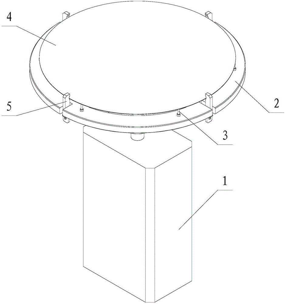
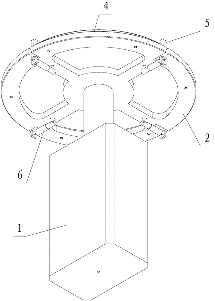
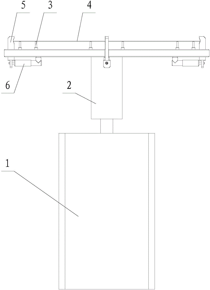
[0021] like Figure 1~5 As shown, the clamping device of the present invention includes a hollow shaft motor 1, a wafer carrier table 2, a pad column 3, a clamping block 5 and a single-acting spring return cylinder 6, wherein the wafer carrier table 2 and the hollow shaft motor 1 The output end of the wafer carrier 2 is sealed and connected. On the upper surface of the wafer carrier 2, there are a plurality of pad columns 3 supporting the edge of the wafer 4 evenly distributed along the circumferential direction. Acting spring return cylinder 6, the output end of each single-acting spring return cylinder 6 is connected with clamping block 5 clamping the edge of wafer 4; The circulation port of the medium, each clamping block 5 reciprocates along the radial direction of the wafer 4 through the expansion and contraction of the single-acting spring return cylin...


PUM


Abstract

The invention relates to a clam device used for wafer cleaning in a semiconductor industry and specifically relates to a device for clamping the edge of a wafer during an automatic wafer cleaning process and a clamping method of device. A wafer bearing table in the device is in sealed connection with the output terminal of a hollow shaft motor. A plurality of gasket posts support the edge of the wafer are distributed on the upper surface of the wafer bearing table in the circumferential direction. A plurality of single-action spring reset cylinder are distributed on the lower surface of the wafer bearing table in the circumferential direction. The output terminal of each single-action spring reset cylinder is connected with a clamp block clamping the edge of the wafer. The wafer bearing table is provided with a flow port used for providing working medium for the single-action spring reset cylinders. When the working medium is not in connection, a piston rod of each single-action spring reset cylinder is in a contraction state, so that the edge of the wafer is clamped tightly. When the working medium is in connection, the piston rod of each single-action spring reset cylinder extends out and the edge of the wafer is released. The device is only in contact with the edge of the wafer and no damage may be caused to the wafer during a technique implementation process.

Description

technical field [0001] The invention relates to a clamping device used for wafer cleaning in the semiconductor industry, in particular to a device and a clamping method for clamping the edge of a wafer when the wafer is automatically cleaned. Background technique [0002] The cleaning process has to be repeated many times in the semiconductor manufacturing process, and the quality of the cleaning effect will largely affect the quality issues such as chip manufacturing process and circuit characteristics. In some cases, both the front and back sides of the wafer need to be cleaned, so that when the other side needs to be cleaned, the cleaned side is not allowed to have external contact except the edge of the wafer. [0003] At present, when doing the wafer cleaning process, there are mainly two ways to pick up the wafer by vacuum adsorption or by eccentric installation of the wafer and the wafer holder. The way of vacuum adsorption inevitably has a large range of contact wit...

Claims


Application Information

Patent Timeline
Patent Type & Authority Applications(China)
IPC IPC(8): H01L21/67H01L21/683
Inventor 李晓飞
Owner SHENYANG KINGSEMI CO LTD
Why Eureka
Try Eureka