IGBT device with high latching resisting capability

A latch and device technology, applied in the field of semiconductor devices, can solve the problems of IGBT device design and process difficulty, large conduction voltage drop of IGBT devices, and insignificant conductance modulation effect, so as to improve the anti-latch ability and reduce conduction. Pressure drop, downsizing effect

Active Publication Date: 2016-07-13
JIANGSU CAS IGBT TECHNOLOGY CO LTD +1
View PDF4 Cites 4 Cited by
  • Summary
  • Abstract
  • Description
  • Claims
  • Application Information

AI Technical Summary

Problems solved by technology

[0005] During specific work, the region part of the P-type heavily doped region 5 located under the N+ source region 4 can form an anti-latch-up structure 11. In order to make the device have high anti-latch-up performance, the P-type anti-latch-up structure 11 is formed The doping concentration must be very high, and at the same time, the high doping must be as close as possible to the sidewall of the cell trench 13, and since the P-type doping of the sidewall of the cell trench 13 directly affects the threshold voltage of the IGBT device, so the The anti-latch-up structure 11 brings great difficulty to the design and process of IGBT devices
[0006] On the other hand, in order to prevent the IGBT device from latch-up during use, the doping concentration of the P-type collector region 9 is generally relatively low, and its junction depth is generally relatively shallow, which makes the holes injected by the N-type base region 7 Relatively small, the conductance modulation effect is not significant, which will lead to a relatively large turn-on voltage drop of the IGBT device

Method used


Image

  • IGBT device with high latching resisting capability
  • IGBT device with high latching resisting capability
  • IGBT device with high latching resisting capability

Examples


Embodiment Construction

[0036] The present invention will be further described below in conjunction with specific drawings and embodiments.

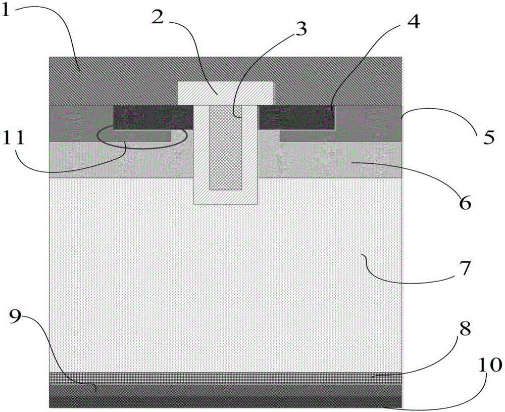
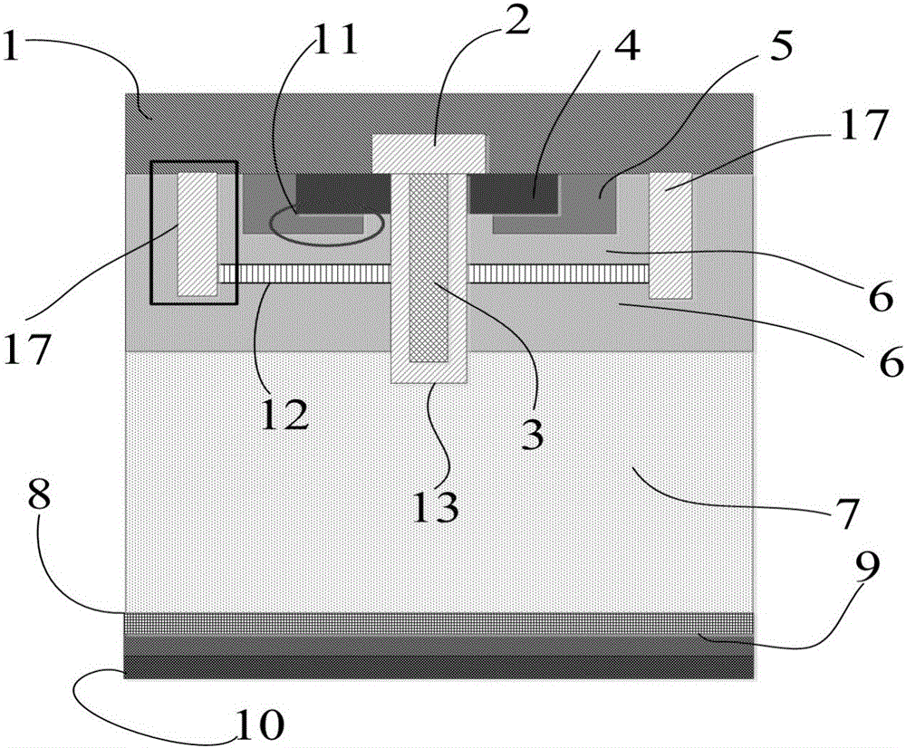
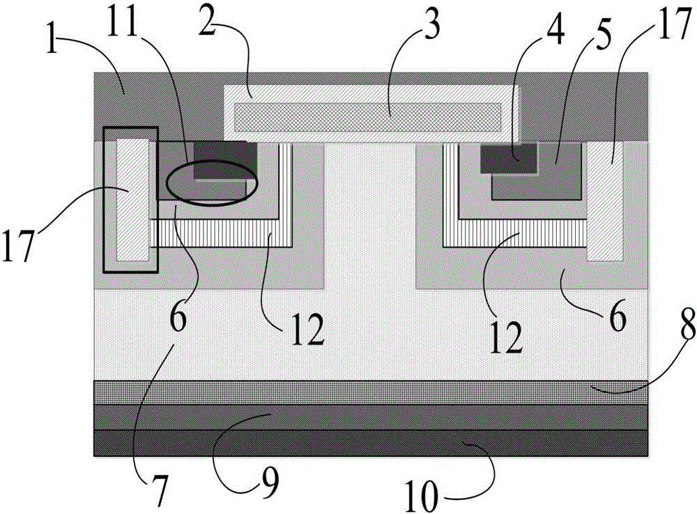
[0037] In order to effectively reduce the risk of latch-up and provide a basis for reducing the conduction voltage drop, taking an N-type IGBT device as an example, the present invention includes a semiconductor substrate with two opposite main surfaces, and the two opposite main surfaces of the semiconductor substrate include the first A main surface and a second main surface corresponding to the first main surface; an N-type base region 7 is included between the first main surface and the second main surface of the semiconductor substrate; several regular rows are arranged in the N-type base region 7 of the semiconductor substrate The active cells 16 distributed parallel to each other, the active cells 16 include the P-type base region 6 located in the upper part of the N-type base region 7 and the N+ source region 4 located in the P-type base region 6 , the ...


PUM


Abstract

The invention relates to an IGBT device with a high latching resisting capability.Each active cell of the IGBT device comprises a second conduction type base region and a first conduction type source electrode region.Barrier rings are arranged in the second conduction type base regions.On the section of the IGBT device, each barrier ring comprises a first conduction type buried layer and an insulating dielectric cylinder, wherein the upper end of the insulating dielectric cylinder makes contact with source electrode metal, the end, located under the corresponding first conduction type source electrode region, of the first conduction type buried layer makes contact with the insulating dielectric cylinder, the other end of the first conduction type buried layer makes contact with the side wall of a conducting channel, the length of the part, under the corresponding first conduction type source electrode region, of the first conduction type buried layer is not smaller than the length of the part, in the corresponding second conduction type base region, of the corresponding first conduction type source electrode region, and the first conduction type buried layer is insulated from the source electrode metal.The IGBT device is compact in structure, compatible with the existing process, safe, reliable and capable of effectively reducing the latching risk and providing a basis for reducing the on-state voltage drop.

Description

technical field [0001] The invention relates to a semiconductor device, in particular to an IGBT device with high latch-up resistance, and belongs to the technical field of IGBT devices. Background technique [0002] There are parasitic thyristors in the IGBT device, that is, the NPNP structure. During normal operation of the device, it is undesirable to turn on the parasitic thyristor. If the parasitic thyristor is turned on, the gate of the IGBT device will lose control of the current. However, during the operation of the IGBT, if the hole current flowing under the source is too large, the PN junction between the source and the base region will be forward biased, that is, the source starts to inject electrons into the base region, and the base region begins to inject electrons into the source region. At this time, the parasitic thyristor is turned on, that is, the IGBT device is in a latched state. [0003] Now that the current density pursued by IGBT is getting higher ...

Claims


Application Information

Patent Timeline
Patent Type & Authority Applications(China)
IPC IPC(8): H01L29/739H01L29/06H01L29/10
CPCH01L29/06H01L29/0607H01L29/1095H01L29/7393
Inventor 杨飞沈千行朱阳军卢烁今田晓丽
Owner JIANGSU CAS IGBT TECHNOLOGY CO LTD
Why Eureka
Try Eureka