A manufacturing method of a current protector and a pcb board
A current protector and PCB board technology, which is applied in the manufacture of fuses, emergency protection devices, emergency protection devices, etc., can solve problems such as looseness and increased cold resistance of fuses, reduce manufacturing costs, and improve resistance accuracy , Good product size consistency
- Summary
- Abstract
- Description
- Claims
- Application Information
AI Technical Summary
Problems solved by technology
Method used
Image
Examples
Embodiment 1
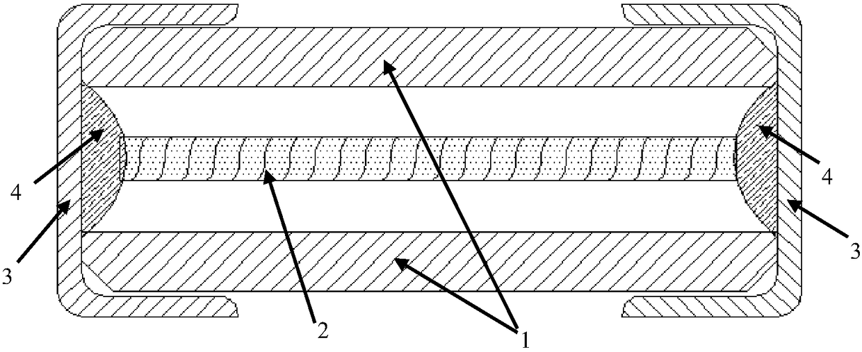
[0023] figure 1 It is a longitudinal sectional view of the ultra-micro current protector according to the present invention. The structure of the protector includes an insulating shell 1 , a metal melt 2 , left and right end caps 3 and solder 4 . Wherein, the molten metal 2 is suspended in the insulating shell 1 , and the solder 4 is fixed and welded to the molten metal 2 inside the end cap 3 to form an electrical connection.
[0024] The PCB board is made of FR-4 material with a heat resistance temperature above 260°C;
[0025] The pressing of the PCB board is to use high-temperature-resistant PCB board adhesive glue on a press to bond two-layer boards under high temperature and high pressure to form a block product.
Embodiment 2
[0027] A kind of manufacture method that is used for the ultra-micro current protector of the present invention:
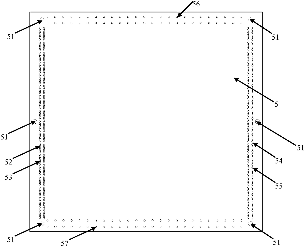
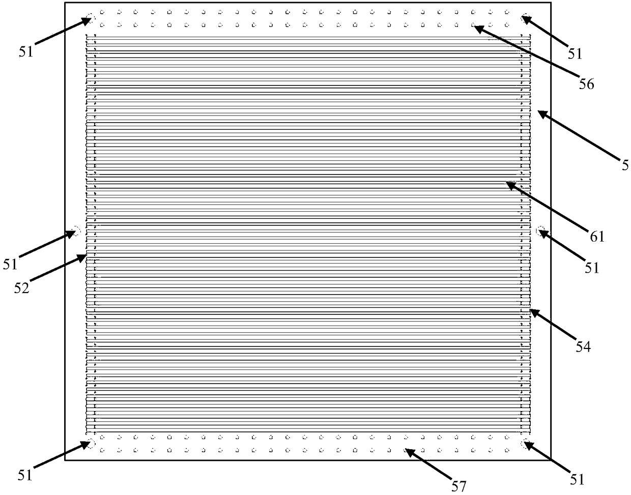
[0028] Two PCB boards are provided, and each PCB board is provided with a pressing alignment hole 51 for pressing and aligning the two PCB boards; and the left side of each PCB board is provided with at least one row of left cutting pairs Positioning holes 52 and at least one row of alignment holes 53 for the left center slot, and at least one row of alignment holes 54 for right cutting and at least one row of alignment holes 55 for right center slot are provided on the right side of each PCB. The alignment holes 52 for left cutting and the alignment holes 54 for right cutting are arranged symmetrically; the alignment holes 53 for the left center groove and the alignment holes 55 for the right center groove are also arranged symmetrically. Among them, the preset left and right center slot alignment holes are prepared for cutting the center slot below, and cutting ...
Embodiment 3
[0037] In step 1 described in Embodiment 2, due to the difference in the field of view of the PCB board cutting machine and the width of the entire PCB board, such as Figure 5 , Figure 6 As shown, the four corners of the upper and lower PCB boards 5 and the middle positions of the sides are punched to form alignment holes 51 for product pressing, and then punched to form alignment holes 51 for product cutting according to the product size at a position in the four sides and the middle of the PCB board 5 . The horizontal both sides and a certain position in the middle of it are punched and formed product central groove aligning hole 59 according to the cutting groove width as the diameter. That is, the PCB board is also provided with a row of auxiliary center slot alignment holes 59 located in the middle of the left center slot alignment hole 53 and the right center slot alignment hole 55; A row of auxiliary cutting alignment holes 58 in the middle of the positioning holes 5...
PUM
 Abstract
Description
Claims
Application Information


