Current protector and manufacturing method
A technology for current protectors and manufacturing methods, which is applied in the direction of emergency protection devices, circuits, electrical components, etc., and can solve problems such as increased cold resistance and looseness of fuses, improve resistance accuracy, reduce manufacturing costs, and reduce product size. good consistency
- Summary
- Abstract
- Description
- Claims
- Application Information
AI Technical Summary
Problems solved by technology
Method used
Image
Examples
Embodiment 1
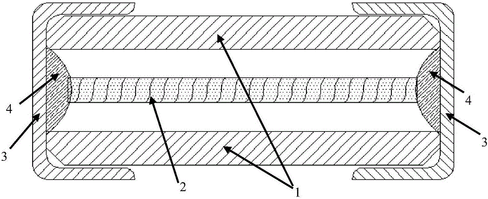
[0026] figure 1 It is a longitudinal sectional view of the ultra-sensitive protector of the present invention, the structure of which includes an insulating shell 1, a metal melt 2, left and right end caps 3 and solder 4. Wherein, the molten metal 2 is suspended in the insulating shell 1 , and the solder 4 is fixed and welded to the molten metal 2 inside the end cap 3 to form an electrical connection.
[0027] and see Figure 8 As shown, the insulating casing 1 includes three layers of PCB boards, and the three layers of PCB boards include two layers of outer PCB boards 11 and a middle PCB board 12 sandwiched between the two layers of outer PCB boards; There is a slot 13 running through the middle PCB, and the slot 13 together with the two outer PCBs 11 forms an inner hole for receiving the molten metal 2 .
[0028] The three-layer PCB boards are all FR-4 materials with a heat-resistant temperature above 260°C;
[0029] The pressing of the three-layer PCB board is to use hi...
Embodiment 2
[0031] A kind of manufacture method that is used for current protector of the present invention:
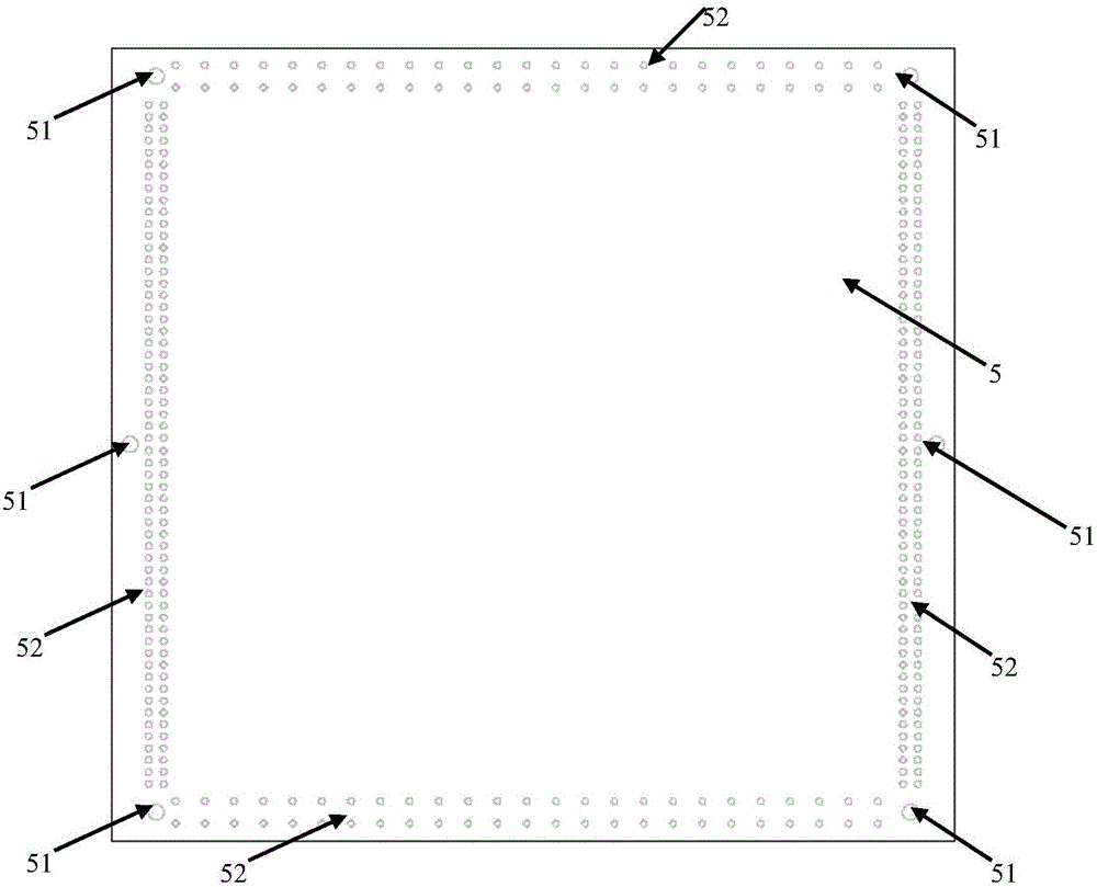
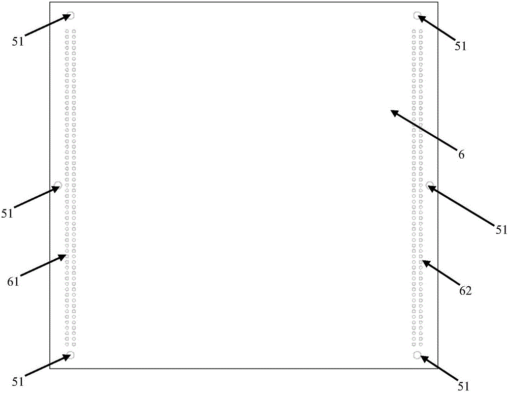
[0032] Three PCB boards are provided, including two outer PCB boards 5 and one inner PCB board 6, and each PCB board is provided with a pressing alignment hole 51 for pressing and aligning the three PCB boards;
[0033] The left side on each outer PCB board 5 is provided with at least one row of alignment holes 52 for left cutting, and the right side of each outer PCB board is provided with at least one row of alignment holes 53 for right cutting; The hole 52 is arranged symmetrically with the alignment hole 53 for right cutting; the upper side of each outer PCB board is provided with at least one row of alignment holes 54 for upper cutting, and the lower side of each outer PCB board is provided with at least one row for lower cutting. alignment holes 55 , and the alignment holes 54 for upper cutting and the alignment holes 55 for lower cutting are arranged symmetrically. The pr...
Embodiment 3
[0041] In step 1 described in Embodiment 2, due to the difference in the field of view of the PCB board cutting machine and the width of the entire PCB board, such as Figure 5 As shown, the four corners of the outer PCB board 5 and the middle positions of the sides are punched to form alignment holes 51 for product pressing, and then punched to form alignment holes 51 for product cutting at a certain position in the four sides and the middle of the outer PCB board 5 according to the product size. That is, the outer PCB 5 is further provided with a row of auxiliary cutting alignment holes 56 located in the middle of the left cutting alignment holes 52 and the right cutting alignment holes 53 . Similarly, a row of center cutting alignment holes 57 located between the upper cutting alignment holes 54 and the lower cutting alignment holes 55 is also provided. Therefore, during size cutting, the cutting alignment can refer to the alignment hole 56 for auxiliary cutting and the ali...
PUM
| Property | Measurement | Unit |
|---|---|---|
| Heat resistance temperature | aaaaa | aaaaa |
Abstract
Description
Claims
Application Information


